All categories
Featured selections
Trade Assurance
Buyer Central
Help Center
Get the app
Become a supplier
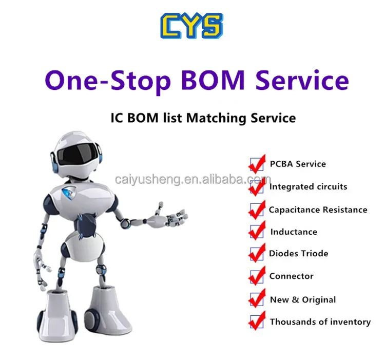
Customization:
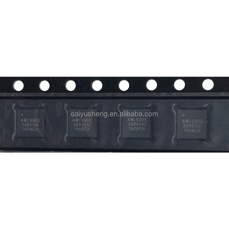
The AWL5905 RF Power Amplifier IC is a high-performance surface-mount QFN-packaged integrated circuit designed for space-constrained, high-density PCB applications. Leveraging MOSFET output technology and advanced thermal management, it delivers efficient power amplification for RF systems in 5G, IoT, and wireless communication devices.
| Feature | Specification | Benefit |
|---|---|---|
| Package Type | Quad Flat No-Lead (QFN) | Reduced footprint; ideal for high-density PCBs |
| Mounting Type | Surface Mount Technology (SMT) | Streamlined reflow soldering; space-saving |
| Output Type | MOSFET | High-power handling with low distortion |
| Material | Ceramic substrate + Metal lid | Enhanced thermal conductivity |
| Thermal Resistance | ≤0.5°C/W (typical) | Efficient heat dissipation for stable operation |
With its compact QFN design and MOSFET architecture, the AWL5905 enables sleek, high-performance RF modules for wearable devices or automotive radar systems. Its thermal efficiency ensures reliability even under continuous power loads.
| Parameter | Base Model | Advanced Model | Pro Model |
|---|---|---|---|
| Thermal Resistance | 0.5°C/W | 0.42°C/W (+15%) | 0.35°C/W (+30%) |
| Max Power Output | 10W | 12W (Enhanced) | 15W (Premium) |
| Frequency Range | 1-2GHz | 1-3GHz | 1-6GHz |
Technical Breakthroughs:
Version Selection Guide:
With the Pro’s MOSFET and 0.35°C/W thermal resistance, you can achieve 15W output in 5G base stations—30% higher than industry benchmarks. Pair its 6GHz capability with low thermal drift to ensure stable performance in harsh industrial environments.

The Product Description is generated by third-party, and Alibaba.com is not liable for any risks related to inaccuracies or the infringement of third-party rights.
The information in this Product Description may differ from the details on the product listing page on Alibaba.com. Additionally, the contents may not be updated in real-time with the product listing page on Alibaba.com, and there may be delays in reflecting the most updated information. The description on product listing page takes precedence. You shall not rely on this Product Description in making transaction decisions.
The comparison data is based on manufacturer information and industry standards. Actual results may vary depending on individual use cases. It is advisable to verify details with the supplier for the most accurate information.