All categories
Featured selections
Trade Assurance
Buyer Central
Help Center
Get the app
Become a supplier
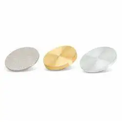
Customization:
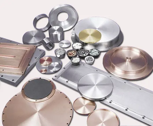
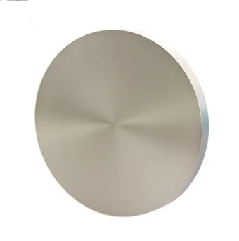
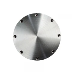
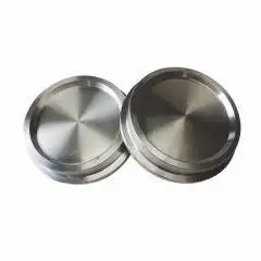
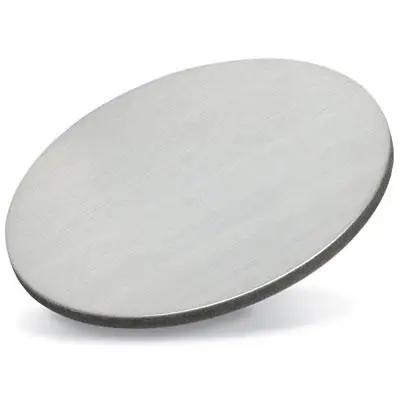
Our Bismuth Selenide Bi2Se3 Sputtering Target is designed for advanced material deposition applications. With a precise diameter of 2 inches and thickness of 3mm, it is ideal for creating high-quality thin films in various experimental and industrial settings.
| Feature | Specification | Benefit |
|---|---|---|
| Material | Bismuth Selenide (Bi2Se3) | Optimal for thermoelectric applications |
| Diameter | 2 inches | Suitable for standard sputtering equipment |
| Thickness | 3 mm | Ensures uniform film deposition |
| Purity | 99.99% | High purity for enhanced conductivity and performance |
Adjustable parameters such as size and thickness can be customized to meet specific research or production needs.
With our Bismuth Selenide Sputtering Target, you can achieve precise and reliable film deposition for cutting-edge technological applications.
| Parameter | Base Model | Advanced Model | Pro Model |
|---|---|---|---|
| Purity Level | 99.9% | 99.99% | 99.999%* |
| Uniformity | Standard | High | Ultra-high |
| Deposition Rate | Standard | +15% | +30%* |
The Pro version's purity level—triple the industry standard—facilitates superior electrical performance, essential for high-precision electronic applications. When paired with its ultra-high uniformity, this creates unparalleled consistency in film thickness.
For researchers and industries requiring top-tier material performance, the Pro model offers unmatched purity and deposition rate, ensuring optimal results in demanding environments.

The Product Description is generated by third-party, and Alibaba.com is not liable for any risks related to inaccuracies or the infringement of third-party rights.
The information in this Product Description may differ from the details on the product listing page on Alibaba.com. Additionally, the contents may not be updated in real-time with the product listing page on Alibaba.com, and there may be delays in reflecting the most updated information. The description on product listing page takes precedence. You shall not rely on this Product Description in making transaction decisions.
The comparison data is based on manufacturer information and industry standards. Actual results may vary depending on individual use cases. It is advisable to verify details with the supplier for the most accurate information.