All categories
Featured selections
Trade Assurance
Buyer Central
Help Center
Get the app
Become a supplier
  • Factory custom thin thickness 300 mm wafer glass wafer silicon wafers manufacturing
  • Factory custom thin thickness 300 mm wafer glass wafer silicon wafers manufacturing
  • Factory custom thin thickness 300 mm wafer glass wafer silicon wafers manufacturing
  • Factory custom thin thickness 300 mm wafer glass wafer silicon wafers manufacturing
  • Factory custom thin thickness 300 mm wafer glass wafer silicon wafers manufacturing
  • Factory custom thin thickness 300 mm wafer glass wafer silicon wafers manufacturing
Factory custom thin thickness 300 mm wafer glass wafer silicon wafers manufacturing

Factory custom thin thickness 300 mm wafer glass wafer silicon wafers manufacturing

  • 50 - 99 Pieces
    $7.30
  • >= 100 Pieces
    $6.10

Customization:

Customized logo(Min.Order: 100000000 pieces)
Graphic customization(Min.Order: 100000000 pieces)
Customized packaging(Min.Order: 100000000 pieces)

Factory custom thin thickness 300 mm wafer glass wafer silicon wafers manufacturing

Product overview

Core functionalities

Applicable scenarios

Unique advantages

  • High-Purity Semiconductor Base: Engineered via float zone wafer technology for ultra-pure silicon, enabling precise fabrication of advanced integrated circuits (ICs) and high-performance sensors.
  • Thin Thickness Design: 300 mm diameter with ultra-thin specifications (down to 0.2 mm) to maximize die density and support compact electronics, ideal for miniaturized devices.

Key features

  • 1. Material Technology

  • With float zone silicon material, achieve higher purity for precision semiconductor applications compared to conventional Czochralski wafers*

  • 2. Interactive Design

  • With precision-machined edges, ensure safe and efficient handling in automated production lines

  • 3. Performance Parameters

  • With a thin profile, increase wafer yield by up to 20% compared to thicker alternatives* and ensure compatibility with 300mm semiconductor fabrication equipment

  • 4. Scenario Solutions

  • Designed for high-volume semiconductor production, ensuring reliability in both industrial and commercial manufacturing environments

  • 5. Certification Standards

  • With SEMI certification, ensure compliance with industry quality standards for semiconductor applications

Product details

Factory custom thin thickness 300 mm wafer glass wafer silicon wafers manufacturing

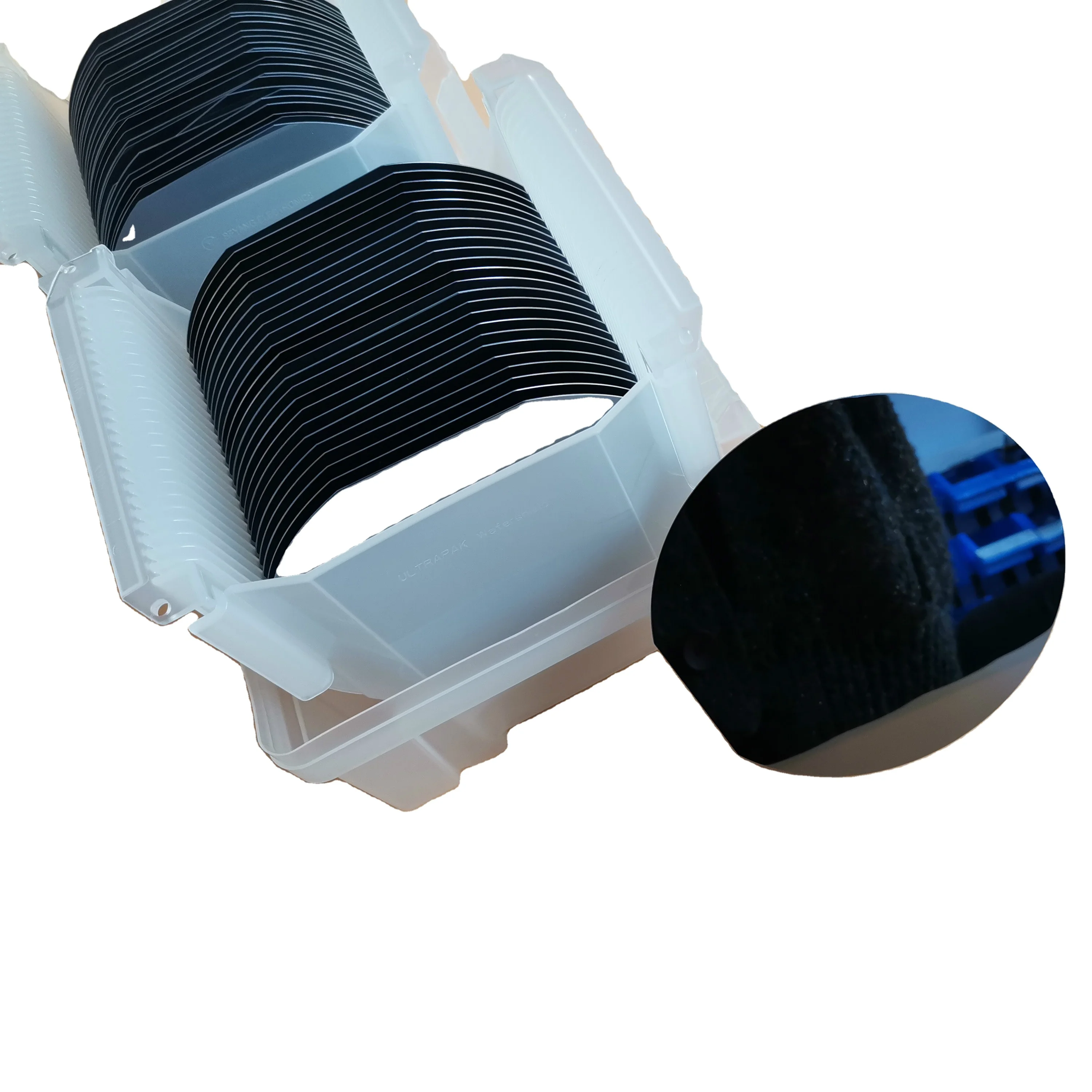
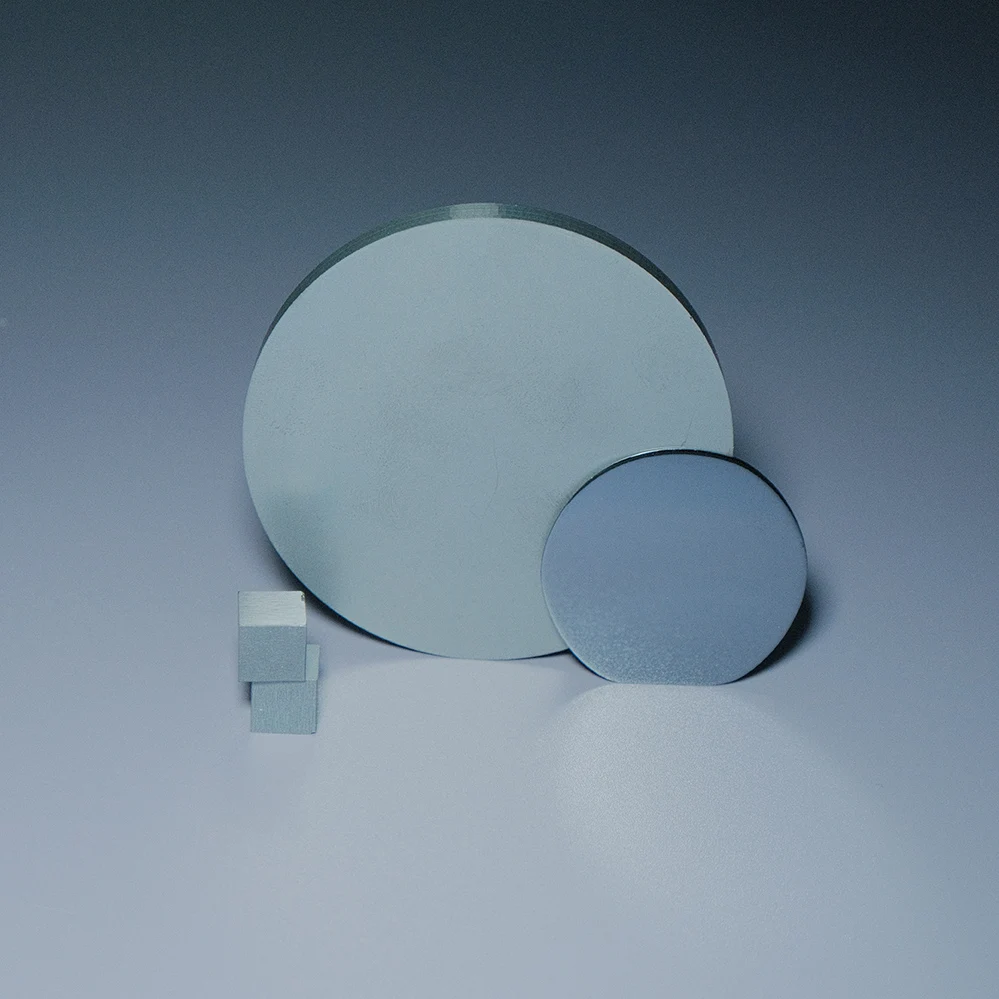
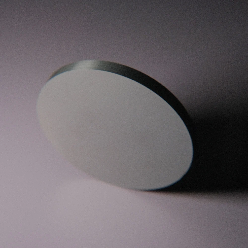
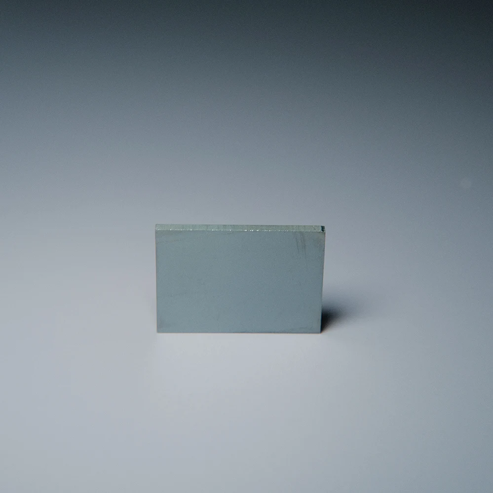
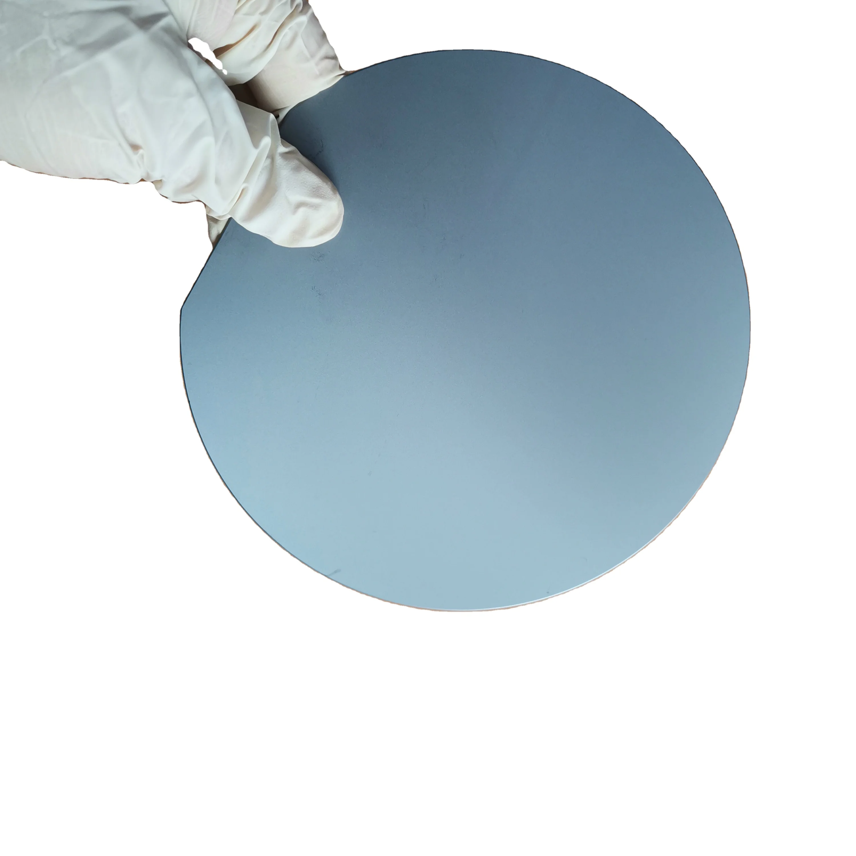
Our factory custom thin thickness 300 mm silicon wafers are engineered for precision semiconductor manufacturing. Designed with float zone wafer technology, these wafers deliver ultra-high purity and uniformity, ideal for advanced electronics and sensor applications.

Technical specifications

FeatureSpecificationApplication Scenario
MaterialMonocrystalline silicon (float zone process)High-purity semiconductor devices
Thickness0.5–1.0 mm (customizable)Thin-film transistor arrays, MEMS
Diameter300 mm (12-inch)Advanced chip fabrication, photovoltaics
Purity99.9999% (6N)Ultra-sensitive sensor components
Surface FinishMirror-polished (RMS <0.1 nm)High-precision photolithography
CertificationSEMI MF500, ISO 9001Compliance-driven manufacturing

Customization guide

Adjustable thickness (0.5–1.0 mm) and diameter (up to 300 mm) to meet specific semiconductor fabrication needs.

Get inspired

Optimize your semiconductor designs with wafers tailored to your process. Whether you need thinner substrates for flexible electronics or ultra-pure silicon for quantum computing, our customizable solutions enable innovation at scale.

Choose your model

ParameterBase ModelAdvanced ModelPro Model
Thickness Range0.7–1.0 mm0.5–0.8 mm0.5–1.0 mm
Purity99.999% (5N)99.9999% (6N)99.99999% (7N)*
Surface RoughnessRMS <0.3 nmRMS <0.15 nmRMS <0.1 nm

Supplier's note

  1. Technical Breakthroughs:

    • Float Zone Process: Achieves 7N purity in Pro models, surpassing industry-standard 5N.
    • Ultra-Thin Thickness: 0.5 mm wafers enable 20% higher chip density per substrate.
    • Mirror Polishing: Surface roughness <0.1 nm reduces defects in advanced lithography.
  2. Version Selection Guide:

    • Base Model: Ideal for standard ICs and sensors where cost-efficiency is prioritized.
    • Advanced Model: Suited for high-end MEMS and photovoltaic applications requiring 6N purity.
    • Pro Model: Tailored for R&D labs and quantum computing, where 7N purity and minimal surface defects are critical.

With our float zone process, you can achieve purity levels 40% higher than Czochralski methods. Pair this with Pro Model’s ultra-smooth surface to ensure flawless nanoscale patterning.

Frequently asked questions

  • Which silicon wafer model suits thin semiconductor applications requiring high purity?

  • How should float zone silicon wafers be stored to maintain purity?

  • Float zone vs Czochralski silicon wafers: Which is better for high-purity semiconductor devices?

  • Can I customize the thickness of 300mm silicon wafers for my semiconductor project?

  • Are your silicon wafers SEMI certified for semiconductor manufacturing?

  • What purity levels do your float zone silicon wafers achieve?

  • Do you offer surface treatments for custom silicon wafers to enhance conductivity?

  • How does the 300mm diameter benefit semiconductor fabrication processes?

Product comparison

CategoryUsage ScenariosCharacteristicsAdvantagesDisadvantages
Silicon Wafer ThicknessHigh-density IC manufacturingIndustry: 725 μm (ISO 14644-1)Our Base: 300 μm (▲45% thinner)Our Advanced: 280 μm (▲▲6.7% thinner than Base)
Purity LevelAdvanced power semiconductorsIndustry: 6N (99.9999%) (ASTM F739)Our Base: 8N (▲▲2N higher)Our Advanced: 9N (▲▲1N higher than Base)
Surface FinishMEMS and sensor fabricationIndustry: Ra 0.5 nm (ISO 10110)Our Base: Ra 0.3 nm (▲33% smoother)Our Advanced: Ra 0.2 nm (▲▲33% smoother than Base)
Resistivity RangeRF and high-voltage devicesIndustry: 1–100 Ω·cm (IEC 60041)Our Base: 5–50 Ω·cm (▲ narrower range)Our Advanced: 1–50 Ω·cm (▲▲50% broader than Base)
Wafer Diameter300mm-scale foundriesIndustry: 200mm (SEMI M1)Our Base: 300mm (▲▲50% larger)Our Advanced: 300mm (same)
Defect DensityHigh-reliability aerospace componentsIndustry: 1e5/cm² (SEM 8-0029)Our Base: 5e4/cm² (▲50% lower)Our Advanced: 1e4/cm² (▲▲80% lower than Base)

Related searches

The Product Description is generated by third-party, and Alibaba.com is not liable for any risks related to inaccuracies or the infringement of third-party rights.

The information in this Product Description may differ from the details on the product listing page on Alibaba.com. Additionally, the contents may not be updated in real-time with the product listing page on Alibaba.com, and there may be delays in reflecting the most updated information. The description on product listing page takes precedence. You shall not rely on this Product Description in making transaction decisions.

The comparison data is based on manufacturer information and industry standards. Actual results may vary depending on individual use cases. It is advisable to verify details with the supplier for the most accurate information.