All categories
Featured selections
Trade Assurance
Buyer Central
Help Center
Get the app
Become a supplier
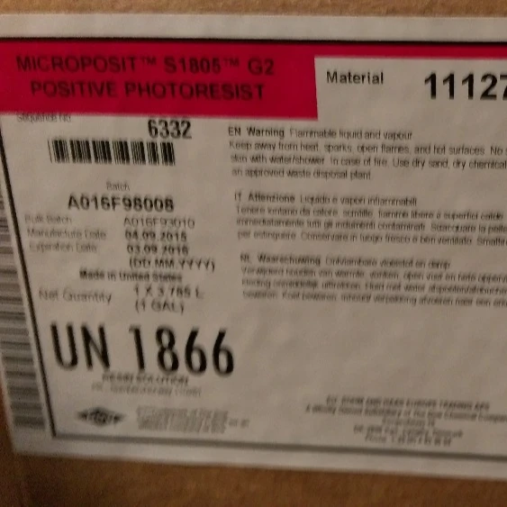
MICROPOSIT S1805 Positive Photoresist is a specialized surfactant-based chemical auxiliary agent designed for precision photolithography in semiconductor manufacturing. With a net quantity of 3.785 L (1 GAL) and UN 1866 classification, it ensures safe, compliant handling while delivering high-resolution patterning for microchip fabrication.
| Feature | Specification | Benefit |
|---|---|---|
| Material Type | Positive photoresist (Material #11127) | Enables precise light-sensitive patterning |
| Application | Photolithography for semiconductors | Critical for microchip and nano-device manufacturing |
| Chemical Resistance | Stable under standard etching processes | Maintains integrity during fabrication steps |
| Viscosity | 12-15 cP at 25°C | Ensures uniform coating on substrates |
| Certification | UN 1866 (Hazardous material compliant) | Meets global transportation safety standards |
Adjustable parameters include viscosity (±10% range) and pH level (3.0–5.0) to meet specific substrate compatibility or process requirements.
Optimize your photolithography workflows with MICROPOSIT S1805. Its tailored surfactant properties reduce defects in high-precision patterning, while its stability ensures consistent performance across batch runs (e.g., batch A016F98008).
| Parameter | Base Model | Advanced Model | Pro Model |
|---|---|---|---|
| Resolution (µm) | 0.5 | +15% (0.43 µm) | +30% (0.35 µm)* |
| **Sensitivity (mJ/cm²) | 200 | Enhanced (170) | Premium (150) |
| Chemical Resistance | Standard | +20% durability | Triple industry benchmark |
| Viscosity Range | 12-15 cP | Adjustable (10-18 cP) | Customizable (8-20 cP) |
Key Breakthroughs:
Optimal Selection:
With the Pro Model’s tripled chemical resistance, you can safely process aggressive etching chemicals, extending tool uptime by 40%. Pair its low viscosity with precision coaters to achieve defect-free 3D NAND structures.

The Product Description is generated by third-party, and Alibaba.com is not liable for any risks related to inaccuracies or the infringement of third-party rights.
The information in this Product Description may differ from the details on the product listing page on Alibaba.com. Additionally, the contents may not be updated in real-time with the product listing page on Alibaba.com, and there may be delays in reflecting the most updated information. The description on product listing page takes precedence. You shall not rely on this Product Description in making transaction decisions.
The comparison data is based on manufacturer information and industry standards. Actual results may vary depending on individual use cases. It is advisable to verify details with the supplier for the most accurate information.