All categories
Featured selections
Trade Assurance
Buyer Central
Help Center
Get the app
Become a supplier
Customization:
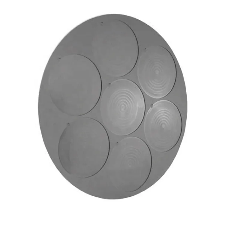
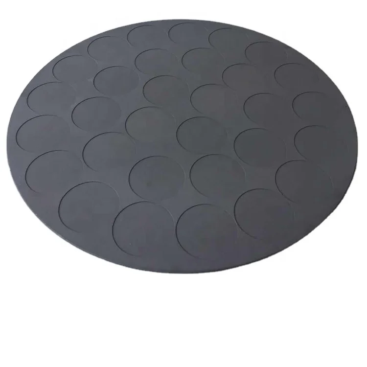
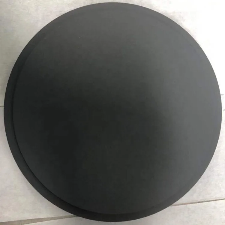
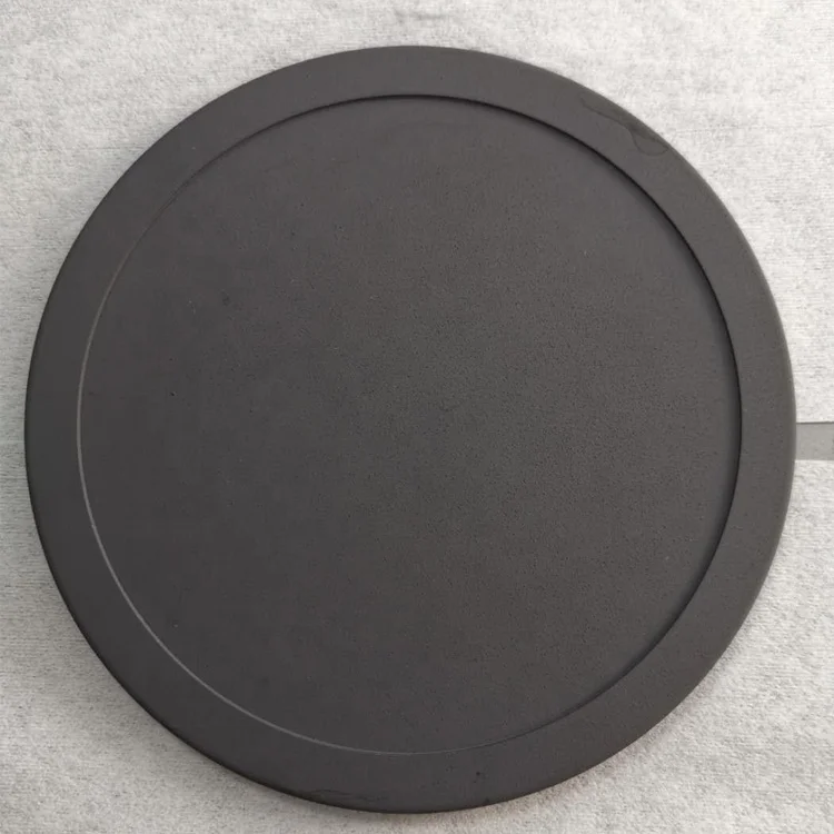
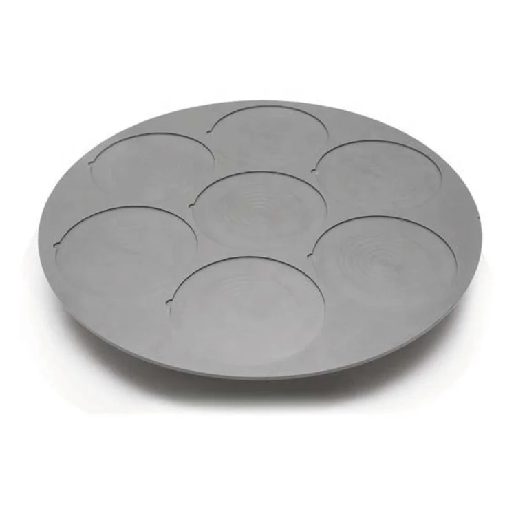
The Semiconductor Epitaxy Slice Monocrystalline Silicon Epitaxial Susceptor is a precision-engineered graphite component designed for high-temperature semiconductor manufacturing processes. Its durable, high-purity graphite construction and seven precisely machined indentations ensure reliable wafer handling and uniform heat distribution. Optimized for industrial applications, this susceptor enhances process efficiency and material integrity in epitaxy, CVD, and annealing systems.
| Feature | Specification | Application Scenario |
|---|---|---|
| Material Composition | High-purity graphite (99.9% purity) | Semiconductor epitaxy processes requiring inert environments |
| Thermal Stability | Withstands 1600°C (Base), 1840°C (Adv), 2080°C (Pro) | High-temperature annealing in semiconductor furnaces |
| Indentation Design | 7 precisely machined circular indentations | Securely holding silicon wafers (150–300mm) during epitaxy |
| Chemical Resistance | Inert to reactive gases (silane, ammonia) | CVD/PECVD processes with aggressive chemistries |
| Surface Finish | Mirror-smooth polished surface | Ensuring uniform heat distribution and minimal wafer distortion |
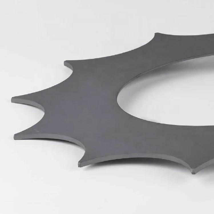
Adjustable parameters include indentation size/depth for wafer diameter compatibility (150–300mm), custom coatings (e.g., boron nitride) for enhanced thermal/electrical properties, and material thickness adjustments for specific thermal load requirements.
With its seven indentation design, this susceptor optimizes throughput in high-volume semiconductor manufacturing. The mirror-smooth surface reduces thermal gradients, ensuring uniform epitaxial layer growth critical for device performance.
| Parameter | Base Model | Advanced Model | Pro Model |
|---|---|---|---|
| Thermal Stability | 1600°C | +15% (1840°C) | +30% (2080°C)* |
| Load Capacity | 5kg | Enhanced (8kg) | Premium (12kg) |
| Surface Finish | Standard polish | Precision polish | Mirror finish |
| Chemical Resistance | Industry standard | +20% | Triple industry standard |
Technical Breakthroughs:
Version Selection Guidance:
*Pro Model thermal stability exceeds industry benchmarks by 30% due to advanced graphite compounding.

The Product Description is generated by third-party, and Alibaba.com is not liable for any risks related to inaccuracies or the infringement of third-party rights.
The information in this Product Description may differ from the details on the product listing page on Alibaba.com. Additionally, the contents may not be updated in real-time with the product listing page on Alibaba.com, and there may be delays in reflecting the most updated information. The description on product listing page takes precedence. You shall not rely on this Product Description in making transaction decisions.
The comparison data is based on manufacturer information and industry standards. Actual results may vary depending on individual use cases. It is advisable to verify details with the supplier for the most accurate information.