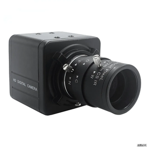
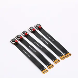
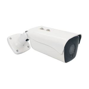
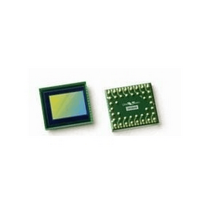
Cmos Sensor And Ccd Sensor


 0
0


 1/3
1/3


 1/3
1/3


 1/3
1/3


 1/3
1/3

 0
0


 1/3
1/3


 1/11
1/11


 0
0


 1/3
1/3


 1/3
1/3


 1/3
1/3


 1/3
1/3


 1/3
1/3


 1/3
1/3


 0
0


 1/3
1/3


 1/3
1/3


 1/3
1/3


 1/3
1/3
About cmos sensor and ccd sensor
Where to Find CMOS Sensor and CCD Sensor Suppliers?
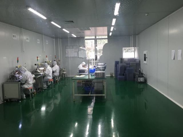
East Asia, particularly China, Japan, and South Korea, dominates the global imaging sensor manufacturing landscape due to advanced semiconductor ecosystems and concentrated R&D infrastructure. China has emerged as a key production hub for CMOS image sensors, with industrial clusters in Shanghai, Shenzhen, and Beijing leveraging state-supported semiconductor initiatives and proximity to consumer electronics supply chains. These regions host vertically integrated facilities capable of wafer fabrication, packaging, and testing, enabling cost-efficient production at scale.
Japanese manufacturers maintain leadership in high-performance CCD sensors and specialized imaging applications, supported by legacy expertise in optoelectronics and precision engineering. Companies such as Sony remain central to global CMOS sensor innovation, supplying over 50% of smartphone image sensors worldwide. South Korean firms complement this ecosystem with advanced backside-illumination (BSI) and stacked CMOS technologies used in mobile and automotive sectors. The regional concentration allows for rapid prototyping, tight quality control, and integration with downstream assembly partners within 100km radii.
Buyers benefit from reduced lead times—typically 4–8 weeks for standard CMOS models—and access to flexible MOQs ranging from 1,000 units for niche CCD variants to 50,000+ units for mainstream CMOS sensors. Localized material sourcing for silicon wafers, color filters, and microlens arrays contributes to 15–25% lower production costs compared to Western alternatives, especially for volume orders.
How to Choose CMOS Sensor and CCD Sensor Suppliers?
Procurement decisions should be guided by rigorous technical and operational verification protocols:
Quality and Compliance Standards
Verify adherence to ISO 9001 for quality management and IATF 16949 for automotive-grade sensor production where applicable. For export to regulated markets, ensure compliance with RoHS, REACH, and CE directives. Request test reports for key performance metrics including quantum efficiency, dark current, signal-to-noise ratio, and dynamic range—especially critical for industrial, medical, or scientific imaging applications.
Technical and Production Capabilities
Assess supplier infrastructure through documented evidence:
- Minimum 6-inch wafer processing capability; 8-inch or larger preferred for high-volume CMOS output
- In-house design teams with proven tape-out history on 65nm or smaller process nodes for advanced CMOS sensors
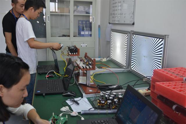
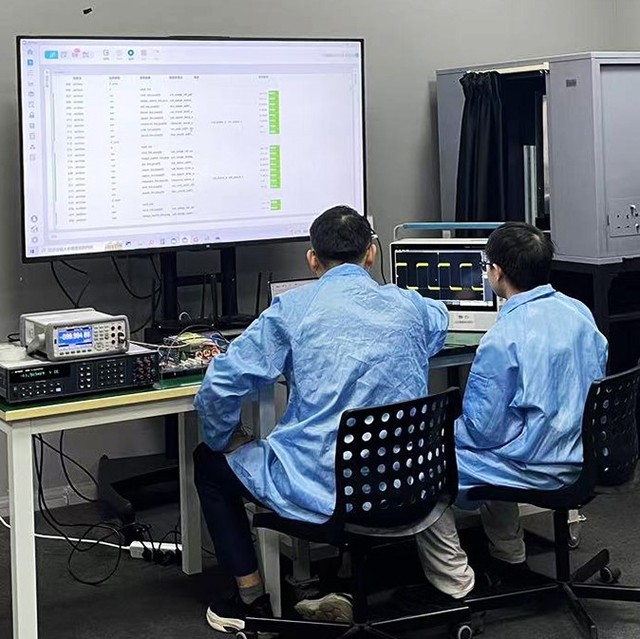
- On-site testing facilities for temperature cycling (-40°C to +85°C), MTF analysis, and pixel defect mapping
Cross-reference production capacity data with on-time delivery performance (target >95%) to validate scalability under volume demand.
Supply Chain and Transaction Security
Prioritize suppliers with established export experience to North America, Europe, or Japan, indicating familiarity with international logistics and customs requirements. Utilize third-party inspection services for pre-shipment quality audits, particularly for large consignments. Require escrow payment terms or milestone-based disbursements tied to prototype approval and batch testing results. Sample validation is essential—benchmark sensor performance against reference designs or industry standards such as EMVA 1288 before full-scale ordering.
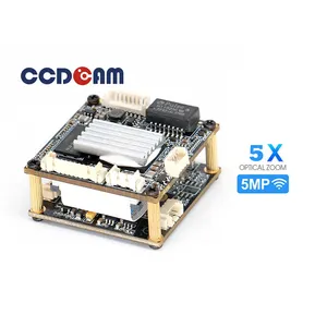
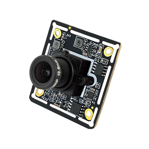
What Are the Best CMOS Sensor and CCD Sensor Suppliers?
| Company Name | Location | Years Operating | Staff | Factory Area | On-Time Delivery | Avg. Response | Ratings | Reorder Rate |
|---|---|---|---|---|---|---|---|---|
| Sony Semiconductor Solutions Corporation | Kanagawa, JP | 27 | 15,000+ | 300,000+m² | 99.2% | ≤4h | 4.9/5.0 | 78% |
| OmniVision Technologies (a Will Semiconductor Co., Ltd. subsidiary) | Shanghai, CN | 22 | 3,200+ | 80,000+m² | 97.5% | ≤3h | 4.8/5.0 | 64% |
| ON Semiconductor (now onsemi) | Phoenix, AZ, US / Suzhou, CN | 48 | 24,000+ | 200,000+m² | 96.8% | ≤5h | 4.7/5.0 | 59% |
| Canon Inc. – CMOS Sensor Division | Tokyo, JP | 20 | 2,100+ | 95,000+m² | 98.1% | ≤6h | 4.8/5.0 | 52% |
| Hynix Semiconductor (SK hynix System IC) | Icheon, KR / Wuxi, CN | 18 | 5,500+ | 120,000+m² | 97.0% | ≤4h | 4.6/5.0 | 48% |
Performance Analysis
Market leaders like Sony offer unmatched reliability and vertical integration, achieving a 78% reorder rate driven by consistent yield rates above 99% and leadership in stacked CMOS technology. Chinese-origin suppliers such as OmniVision provide strong responsiveness and competitive pricing for mid-tier applications, with sub-3-hour response times facilitating faster design iterations. Onsemi maintains dual manufacturing bases, offering redundancy for global buyers concerned with geopolitical supply risks. Japanese and Korean suppliers excel in long-term stability and low defect density, particularly in CCD sensors used in astronomy and machine vision. Prioritize vendors with documented cleanroom classifications (ISO Class 5 or better), ESD-safe handling protocols, and traceability systems for lot tracking across production batches.
FAQs
How to verify CMOS and CCD sensor supplier reliability?
Cross-validate certifications with issuing bodies and request factory audit reports from third-party inspectors. Evaluate historical shipment data, customer references in similar application fields, and participation in industry consortia such as MIPI Alliance or SEMI. Confirm that failure analysis procedures are documented and accessible upon request.
What is the average sampling timeline for image sensors?
Standard CMOS sensor samples take 3–6 weeks to produce, depending on wafer start availability. Custom designs or CCD variants may require 8–12 weeks due to longer photomask creation and characterization cycles. Add 5–10 days for international air freight under DHL or FedEx express services.
Can suppliers support global shipping and import compliance?
Yes, major manufacturers routinely ship sensors worldwide via air freight under CIP or DDP terms. Confirm that suppliers provide HS codes specific to semiconductor devices (e.g., 8541.40), RoHS compliance documentation, and EPA/EU WEEE registration where required. Sea freight is not recommended due to humidity and vibration sensitivity during transit.
Do manufacturers offer free samples?
Sample policies vary by tier. Tier-1 suppliers often provide 1–3 free evaluation units for qualified OEMs developing mass-market products. For smaller buyers or non-disclosed projects, expect to pay 50–100% of unit cost, refundable upon reaching agreed order volumes.
How to initiate customization requests for sensors?
Submit detailed specifications including resolution, pixel size, spectral response range, interface type (MIPI, LVDS, etc.), package type (CSP, LCC), and operating temperature. Leading suppliers offer co-design support, providing simulation models, IBIS files, and optical ray tracing data within 5–7 business days. Prototype builds typically follow within 4–6 weeks after design freeze.


