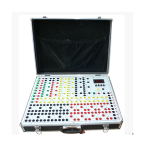
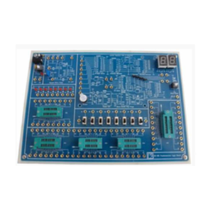
Digital And Logic Design


 1/3
1/3


 1/3
1/3


 1/3
1/3

 CN
CN


 0
0


 1/27
1/27


 1/3
1/3


 1/1
1/1


 1/3
1/3


 1/3
1/3


 1/3
1/3


 0
0


 1/3
1/3


 1/3
1/3


 1/3
1/3


 1/12
1/12


 1/3
1/3


 1/2
1/2


 1/1
1/1


 1/3
1/3
About digital and logic design
Where to Find Digital and Logic Design Suppliers?
Digital and logic design services are primarily concentrated in technology-driven manufacturing hubs across East Asia, with China, Taiwan, and South Korea hosting the most developed ecosystems for semiconductor design, integrated circuit (IC) development, and embedded systems engineering. Within China, industrial clusters in Shanghai, Shenzhen, and Beijing dominate due to proximity to research institutions, semiconductor fabs, and electronics supply chains. These regions support a dense network of design houses, EDA (Electronic Design Automation) tool providers, and testing laboratories, enabling rapid prototyping and scalable production.
The sector benefits from vertically integrated capabilities—many suppliers offer full-turnkey solutions from schematic capture and PCB layout to FPGA programming and ASIC verification. This integration reduces time-to-market by up to 40% compared to fragmented outsourcing models. Buyers gain access to specialized talent pools, with over 75% of leading firms employing engineers certified in Verilog, VHDL, and SystemC. Average lead times for functional prototypes range from 21–35 days, depending on complexity, while batch production cycles for validated designs typically run 30–60 days post-approval.
How to Choose Digital and Logic Design Suppliers?
Prioritize these verification protocols when selecting partners:
Technical Compliance
Confirm adherence to IEEE 830 (software requirements), IEC 61508 (functional safety), and IPC-2221 (PCB design standards). For automotive or industrial applications, ISO 26262 or IEC 61131-3 compliance is essential. Request documentation of simulation results, timing analysis reports, and test coverage metrics (e.g., >95% fault coverage in ATPG testing).
Engineering Capability Audits
Evaluate technical infrastructure and workforce qualifications:
- Minimum 8+ years of experience in digital system architecture
- Proficiency in industry-standard tools: Cadence Virtuoso, Synopsys Design Compiler, Xilinx Vivado, or Mentor Graphics ModelSim
- In-house verification environments using UVM/OVM methodologies
Validate project portfolios with FPGA-to-ASIC migration case studies and low-power optimization benchmarks (e.g., dynamic voltage scaling, clock gating).
Intellectual Property & Transaction Safeguards
Require signed NDAs and IP ownership clauses prior to engagement. Verify secure data handling practices, including encrypted file transfer and restricted access to design repositories. Assess version control systems (Git/SVN) and change management protocols. For high-value projects, consider milestone-based payments with deliverable validation at each phase—schematic review, layout completion, and post-silicon testing.
What Are the Best Digital and Logic Design Suppliers?
No supplier data available for comparative analysis.
Performance Analysis
In absence of specific supplier profiles, procurement focus should remain on validating technical depth, process maturity, and export compliance. Leading design firms typically maintain CMMI Level 3 or higher processes, ensuring repeatable workflows and traceability across design phases. Prioritize suppliers with proven experience in target application domains—such as consumer electronics, telecommunications, or automotive ADAS—to minimize integration risks. For customization-heavy projects, confirm availability of RTL code reuse libraries and hardware description language (HDL) templates to accelerate development cycles.
FAQs
How to verify digital and logic design supplier reliability?
Review third-party audit reports on quality management systems (ISO 9001, TL 9000). Validate past project success through client references, focusing on first-pass silicon yield rates and post-deployment bug resolution timelines. Confirm participation in global design alliances or foundry partnerships (e.g., TSMC, SMIC) as indicators of technical credibility.
What is the average sampling timeline?
Functional FPGA prototypes can be delivered within 15–25 days after specification finalization. Full ASIC tape-out cycles require 6–12 weeks, including synthesis, place-and-route, DFT insertion, and GDSII output. Add 2–4 weeks for external fabrication and packaging if not managed in-house.
Can suppliers ship designs worldwide?
Yes, reputable firms support global collaboration via secure cloud platforms and comply with international export controls (e.g., Wassenaar Arrangement for dual-use technologies). Physical delivery applies only to evaluation boards or reference modules; core design assets are transferred electronically under strict licensing terms.
Do manufacturers provide free samples?
Design concept validations or partial HDL code demonstrations may be offered at no cost to qualify engagements. Full design packages require paid contracts, typically structured as fixed-fee milestones or time-and-materials billing. Waivers are rare due to high intellectual labor content.
How to initiate customization requests?
Submit detailed specifications including target technology node (e.g., 28nm, 65nm), power budget, clock frequency, interface standards (PCIe, USB, SPI), and environmental ratings. Reputable suppliers respond with feasibility assessments within 5–7 business days and provide initial architectural block diagrams within 10 days.


