Silicon Wafer Semiconductor


 0
0


 1/49
1/49


 0
0

 CN
CN


 1/3
1/3


 1/3
1/3


 1/3
1/3


 1/3
1/3


 0
0

 0
0


 1/3
1/3


 1/2
CN
1/2
CN


 1/1
1/1


 1/13
1/13


 1/3
1/3


 1/2
1/2

 1/3
1/3


 1/3
1/3


 1/3
1/3


 1/3
1/3

About silicon wafer semiconductor
Where to Source Silicon Wafer Semiconductor Suppliers?
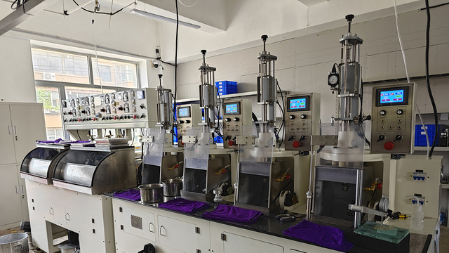
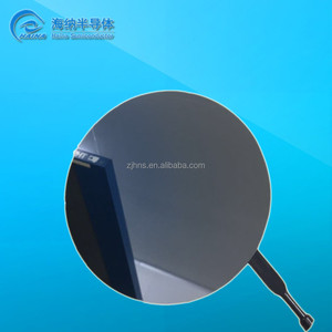
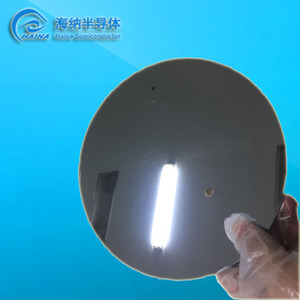
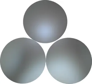
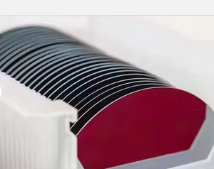
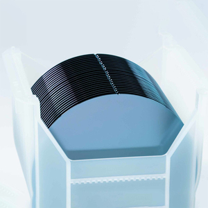
China remains a central hub for silicon wafer semiconductor production, with key manufacturing clusters in Fujian, Henan, Jilin, and Tianjin offering specialized capabilities in monocrystalline and polycrystalline wafer fabrication. These regions host vertically integrated facilities equipped for full-cycle processing—from crystal growth and slicing to polishing and metrology—supporting both IC-grade and optical-grade specifications. Suppliers leverage proximity to raw material sources and regional technical universities to maintain cost efficiency and innovation in high-resistivity, NTD (neutron-transmutation-doped), and epitaxial wafer technologies.
The ecosystem enables scalable production across wafer diameters from 1-inch (25.4mm) to 12-inch (300mm), with multiple vendors capable of handling low-volume R&D orders as well as bulk procurement. Lead times typically range from 15–30 days depending on customization level, while localized supply chains reduce logistics overhead by up to 25% compared to non-Asian manufacturers. Buyers benefit from flexible MOQ structures, online transaction support, and increasing availability of custom doping, orientation (e.g., <100>, <111>), and surface finish options.
How to Evaluate Silicon Wafer Semiconductor Suppliers?
Procurement decisions should be guided by objective evaluation criteria focused on technical compliance, production reliability, and transaction security:
Quality Assurance Standards
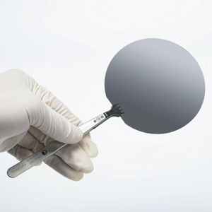
Confirm adherence to international semiconductor quality benchmarks such as ASTM F723 and SEMI standards. While formal ISO 9001 certification is not explicitly stated in available data, prioritize suppliers demonstrating consistent on-time delivery (≥96%) and verifiable process controls. For critical applications, request test reports covering resistivity, thickness tolerance (±0.5μm), total thickness variation (TTV), and surface roughness (Ra ≤0.5nm).
Manufacturing & Customization Capability
Assess supplier infrastructure based on product range and customization indicators:
- Support for wafer sizes up to 300mm indicates advanced processing lines
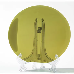
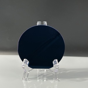
- Offerings in P-type, N-type, SSP/DSP, and high-resistivity (>1000 Ω·cm) wafers reflect material science expertise
- Customization tags suggest capability in laser marking, packaging configuration, and doping profile tuning
Cross-reference breadth of diameter offerings with minimum order flexibility to identify partners suitable for prototyping versus volume deployment.
Order & Transaction Metrics
Analyze operational performance using available KPIs:
- On-time delivery rates above 96% correlate with stable production scheduling
- Response times under 3 hours indicate responsive customer engineering support
- Reorder rates below 19% may reflect niche market positioning or limited repeat application fit
Use online revenue tiers (e.g., >$140K annually) as proxies for export experience and market validation.
Sourcing Safeguards
Implement risk mitigation protocols: require sample testing before full commitment, confirm packaging methods to prevent micro-scratches during transit, and utilize secure payment mechanisms. Insist on clear documentation of wafer grade (prime, test, dummy, reclaimed) and metrology data per lot.
What Are the Leading Silicon Wafer Semiconductor Suppliers?
| Company Name | Main Products | Verified Type | Online Revenue | On-Time Delivery | Avg. Response | Reorder Rate | Sample MOQ | Price Range (USD) |
|---|---|---|---|---|---|---|---|---|
| Xiamen Yingfei Connection Technology Co., Ltd. | Semiconductors, Connectors, Cables | - | $5,000+ | 100% | ≤1h | <15% | 10 units | $4.50–95.00 |
| Nanyang Jingliang Photoelectric Co., Ltd. | Silicon Wafers, Optoelectronics | Custom Manufacturer | $140,000+ | 96% | ≤2h | 19% | 5 pieces/boxes | $150.00 (fixed) |
| Changchun Elink Technology Co.,Ltd. | Semiconductors, MEMS, Solar Panels | - | $30,000+ | 100% | ≤3h | <15% | 5–25 pieces | $0.69–35.99 |
| Zhengzhou Cy Scientific Instrument Co., Ltd. | Silicon Wafers, Thin Film Systems | Custom Manufacturer | $40,000+ | 50% | ≤4h | <15% | 1 blade | $7.00–40.00 |
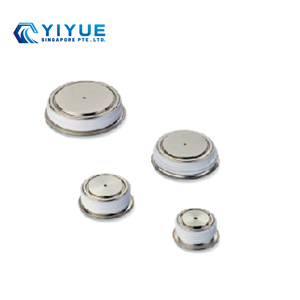
| Tianjin Century Electronics Co., Ltd. | Semiconductors, Thyristors, Diodes | - | Not specified | 100% | ≤3h | Not available | 50–200 pieces | $1.50–46.00 |
Performance Analysis
Xiamen Yingfei and Changchun Elink demonstrate strong logistical reliability with 100% on-time delivery and sub-3-hour response times, making them suitable for time-sensitive procurement. Nanyang Jingliang stands out with the highest reported annual online revenue ($140K+), indicating robust export activity and potential scalability for large orders. Its fixed pricing model at $150 per batch suggests standardized packaging or testing services included in the cost.
Zhengzhou Cy Scientific Instrument offers the lowest entry MOQ (1 blade) but has a significantly lower on-time delivery rate (50%), signaling potential fulfillment risks despite broad customization capabilities in coating and sputtering processes. Tianjin Century Electronics provides competitive pricing down to $1.50/unit with high-volume MOQs, ideal for cost-driven industrial applications.
Buyers seeking IC-grade or MEMS-compatible wafers should prioritize suppliers listing precise specifications such as "IC Grade," "Double-sided Polished," or "Monocrystalline." For R&D use, small-batch availability and low MOQs (e.g., 5–10 units) are critical; for production scaling, verify consistency across batches and audit packaging integrity to minimize yield loss.
FAQs
How to verify silicon wafer quality before purchase?
Request detailed specifications including crystal orientation, dopant type (P/N), resistivity range, thickness, and surface finish. Ask for sample certificates of conformance or third-party inspection reports if available. Conduct incoming inspections for TTV, warp, and particle count upon receipt.
What is the typical lead time for silicon wafer orders?
Standard orders typically ship within 15–25 days. Customized wafers involving special doping, coatings, or packaging may require 30–45 days. Confirm production schedules directly with suppliers prior to order placement.
Can suppliers provide free samples?
Free samples are uncommon due to material and processing costs. Most suppliers charge full or partial price for initial units. Some may credit sample fees against future bulk orders exceeding predefined thresholds.
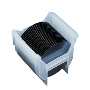
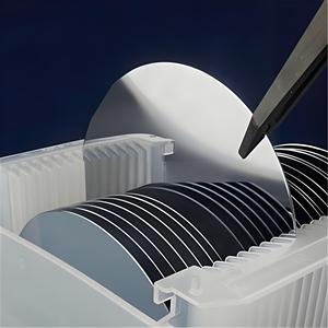
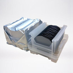
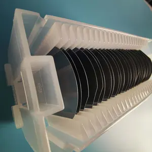
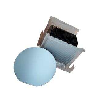
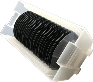
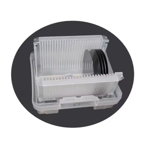
What are common packaging standards for silicon wafers?
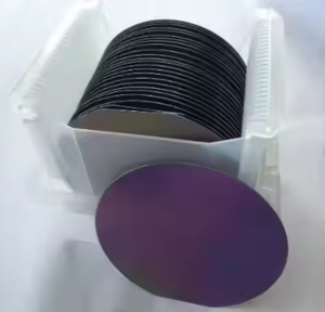
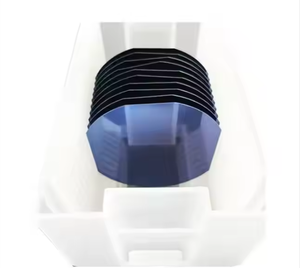
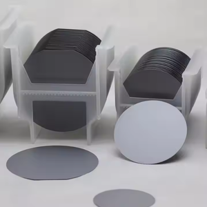
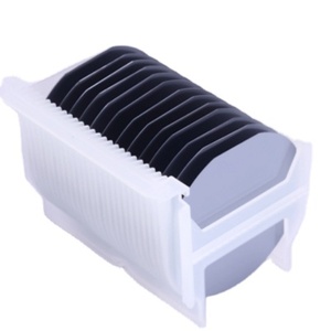
Wafers are typically shipped in sealed cassettes inside antistatic containers with desiccants to prevent moisture and particulate contamination. For fragile or ultra-thin substrates, vacuum-sealed or foam-lined packaging is recommended.
Are custom doping or orientation options available?
Yes, several suppliers list capabilities in P-type, N-type, and high-resistivity configurations. Orientation-specific wafers (<100>, <111>) are commonly offered. Confirm availability of FZ (Float Zone) or CZ (Czochralski) growth methods for specialized applications.


