
Creating a clear and accurate circuit diagram is the foundation of any successful electronics project. Whether you're building a simple LED circuit or planning a complex control system, a well-drawn schematic communicates your design intent precisely and prevents costly errors. For beginners, the process can seem intimidating—filled with unfamiliar symbols, conventions, and terminology. But with a structured approach, anyone can learn to draft professional-quality circuit diagrams.
This guide walks through each essential phase of creating reliable schematics, from understanding basic components to organizing your layout for clarity and functionality. By following these steps, you'll develop diagrams that are not only correct but also easy to troubleshoot, share, and modify.
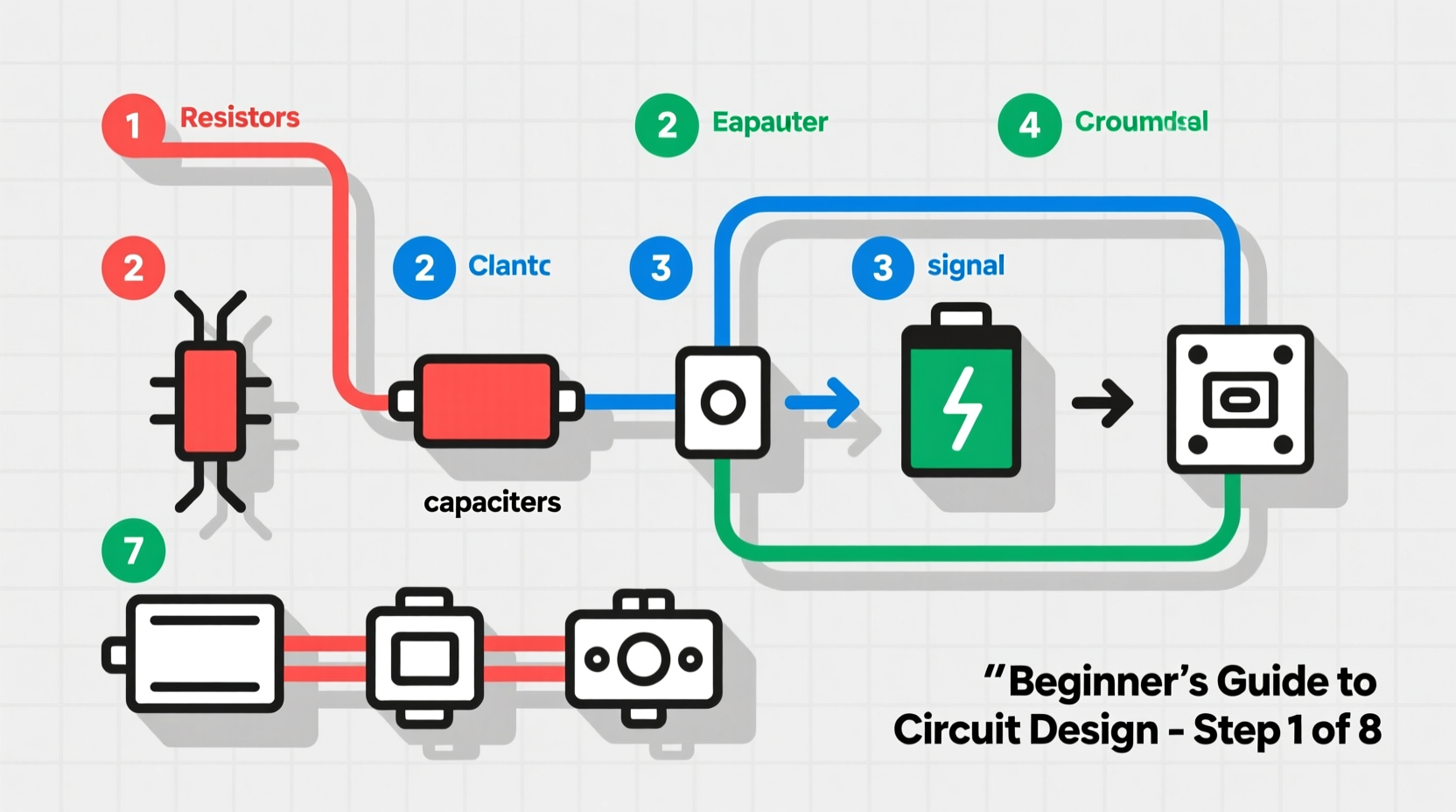
Understand the Purpose and Components of Circuit Diagrams
A circuit diagram, also known as a schematic, is a visual representation of an electrical circuit using standardized symbols instead of realistic images. Unlike wiring or physical layout diagrams, schematics focus on logical connections rather than spatial arrangement. This abstraction allows engineers and hobbyists to analyze circuit behavior without being distracted by physical constraints.
Every symbol in a schematic has a specific meaning:
- Resistor: A zigzag line representing opposition to current flow.
- Capacitor: Two parallel lines (non-polarized) or one curved and one straight (polarized).
- Transistor: Three-terminal devices like NPN or PNP BJTs, shown with emitter, base, and collector lines.
- Integrated Circuits (ICs): Represented as rectangles with labeled pins.
- Power Sources: Batteries (long and short parallel lines), voltage supplies (+Vcc), and grounds (downward-pointing triangles or horizontal lines).
Familiarity with these symbols is non-negotiable. Beginners should spend time studying common representations before attempting to draw full circuits.
Step-by-Step Guide to Building Your First Schematic
Designing an accurate circuit diagram isn’t just about placing symbols—it’s about logical organization, consistency, and attention to detail. Follow this timeline to ensure accuracy at every stage:
- Define the Circuit Function: Start by clearly stating what the circuit should do (e.g., \"light an LED when a button is pressed\"). Write down input, output, and intermediate stages.
- List Required Components: Based on your function, list all necessary parts—resistors, capacitors, ICs, switches, etc.—including values where applicable.
- Select a Drawing Tool: Use software such as KiCad, Fritzing, EasyEDA, or even pen and paper for simple designs. Digital tools offer error checking and netlist generation.
- Draw Power Rails First: Place V+ and ground symbols early. Most schematics orient positive supply at the top and ground at the bottom.
- Place Key Components: Position central elements like microcontrollers, op-amps, or transistors first. Then connect supporting components around them.
- Connect Nodes Logically: Draw wires between component terminals. Avoid crossing lines unnecessarily; use junction dots when connections intersect.
- Label Everything Clearly: Include part values (e.g., R1 = 220Ω), reference designators (R1, C2, U3), and net names (RESET, CLK_OUT).
- Review for Errors: Check continuity, polarity, and missing connections. Ensure no floating inputs or unintended shorts.
Real Example: Designing a Basic LED Blinker
Imagine you want to create a circuit that blinks an LED using a 555 timer IC in astable mode. You begin by identifying the required components: 555 IC, two resistors (R1, R2), a capacitor (C1), an LED, and a current-limiting resistor (R3). After sketching the 555 symbol, you place R1 between pin 7 (discharge) and V+, R2 between pins 6 and 7, and C1 from pin 6 to ground. The output (pin 3) connects to the LED via R3. Finally, you link pin 4 (reset) to V+ and pin 5 to ground through a small capacitor. Every connection follows the standard 555 astable configuration, ensuring predictable oscillation.
“Clarity in schematics saves hours in debugging. A good diagram should make the circuit’s operation obvious at a glance.” — Dr. Alan Reyes, Electrical Engineering Educator
Best Practices for Layout and Readability
An accurate circuit diagram must be both technically correct and visually intuitive. Even if the connections are perfect, poor layout can lead to confusion or mistakes during assembly.
| Do | Don't |
|---|---|
| Use consistent symbol styles across the diagram | Mix different symbol sets (e.g., US vs. European resistor symbols) |
| Route signals from left to right, top to bottom | Create loops or backward signal flows without explanation |
| Group related components together (e.g., power supply section) | Scatter connected parts far apart without labeling nets |
| Add notes or annotations for non-obvious behaviors | Assume others will understand undocumented design choices |
Critical Checklist Before Finalizing Your Diagram
Before sharing or using your schematic for PCB design, run through this checklist to catch common oversights:
- ✅ All components have reference designators (R1, C2, etc.)
- ✅ Component values are clearly marked (10kΩ, 100µF, etc.)
- ✅ Power and ground symbols are correctly placed and labeled
- ✅ No unconnected pins (especially on ICs—tie unused ones appropriately)
- ✅ Polarized components (diodes, electrolytic caps) show correct orientation
- ✅ Wires that cross without connecting use “no connect” markers or hops
- ✅ Net labels are used consistently for multi-sheet or large designs
- ✅ The entire circuit aligns with the intended functionality
Common Pitfalls and How to Avoid Them
Beginners often make subtle but critical errors that compromise the usability of their diagrams. One frequent mistake is omitting ground connections—even though they seem obvious, every circuit must have a defined return path. Another issue is incorrect pinouts; copying a symbol without verifying its pin configuration (e.g., swapping emitter and collector on a transistor) leads to non-functional builds.
Also, overcomplicating the layout by cramming too many components into a small space reduces readability. Instead, break complex systems into functional blocks: power supply, signal processing, output stage, etc. Use hierarchical sheets if your tool supports them.
“Half the troubleshooting time in electronics comes from ambiguous schematics. Invest time upfront to save days later.” — Lila Chen, Embedded Systems Designer
FAQ
What's the difference between a circuit diagram and a wiring diagram?
A circuit diagram shows the logical relationships between components using abstract symbols, while a wiring diagram depicts the physical layout and actual wire paths used in assembly. Schematics are used for design and analysis; wiring diagrams guide construction.
Can I draw circuit diagrams by hand?
Yes, especially for learning or quick prototyping. However, hand-drawn schematics must follow standard symbols and maintain neatness. For serious projects, digital tools provide better accuracy, reuse, and integration with simulation or PCB software.
How do I verify my circuit diagram is correct?
You can simulate it using free tools like LTspice or Tinkercad Circuits. Simulation helps validate functionality before building. Additionally, peer review—having another person check your schematic—is one of the most effective ways to catch errors.
Master the Art of Clear Technical Communication
Designing accurate circuit diagrams is more than a technical skill—it’s a form of communication. A well-crafted schematic tells a story: how electricity flows, how signals are processed, and how components interact. When done right, it becomes a universal language understood by engineers, technicians, and makers worldwide.
Start simple. Practice with basic circuits. Review your work critically. Over time, you’ll develop an eye for clarity and precision that elevates your entire design process. Whether you're preparing for a school project, a personal build, or a professional prototype, mastering schematic design gives you a powerful advantage.


 浙公网安备
33010002000092号
浙公网安备
33010002000092号 浙B2-20120091-4
Comments
No comments yet. Why don't you start the discussion?