All categories
Featured selections
Trade Assurance
Buyer Central
Help Center
Get the app
Become a supplier
Customization:
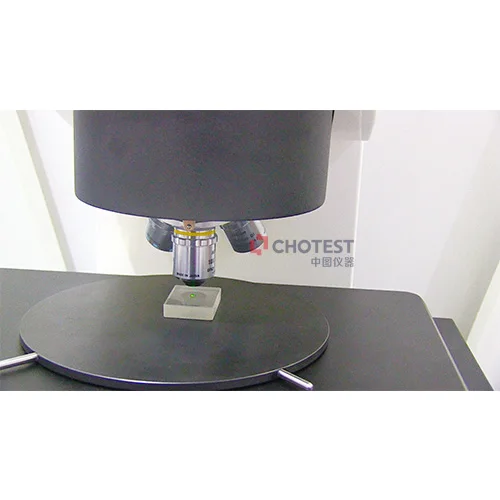
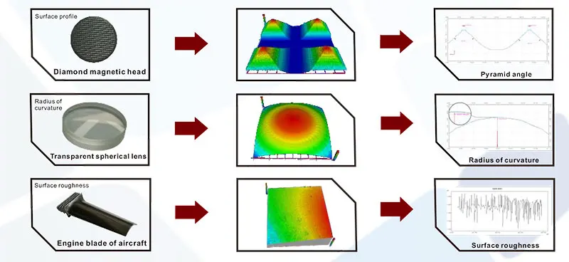
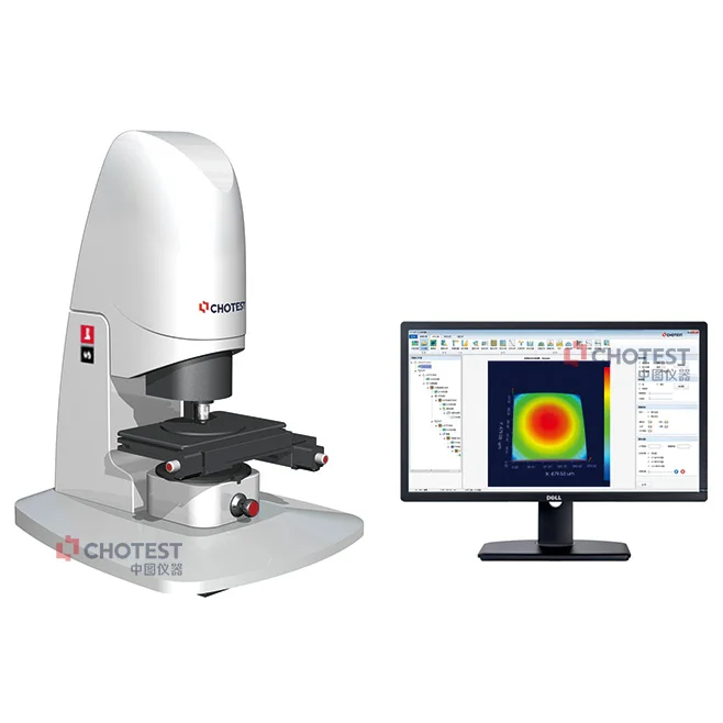
The CHOTEST Non-contact White Light Interferometer is a high-precision optical instrument designed for nano-scale 3D contour and form measurement. With a sleek, ergonomic design and advanced automation, it delivers accurate surface analysis for applications in aerospace, automotive, and medical device manufacturing.
| Feature | Specification | Benefit |
|---|---|---|
| Non-contact Measurement | White Light Interferometry | Analyze delicate surfaces without damage |
| Material Composition | Plastic, metal, and hybrid metal-plastic components | Lightweight yet durable construction |
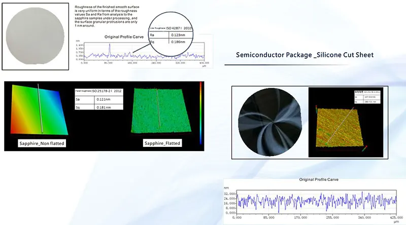
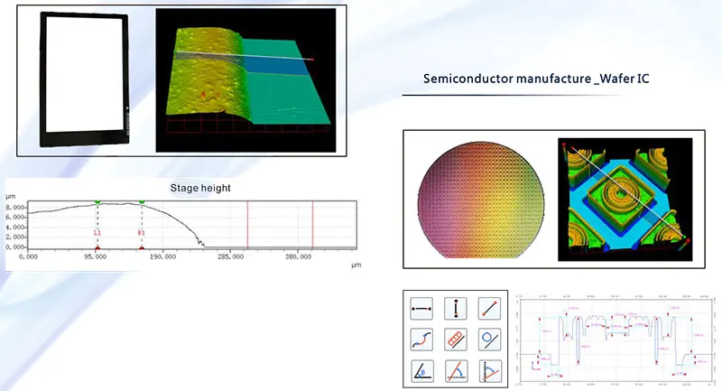
| Precision | ±0.5 nm resolution | Nano-scale accuracy for critical tasks |
| Automation Level | Programmable scan protocols | Streamlined workflows and repeatability |
| Software Interface | User-friendly GUI with 3D surface maps | Intuitive data visualization and analysis |
| Warranty | 1-year manufacturer warranty | Comprehensive coverage for peace of mind |
Adjustable parameters such as measurement resolution, scan area, and sensor sensitivity can be tailored to meet specialized needs like micro-structure inspection or high-volume production quality control.
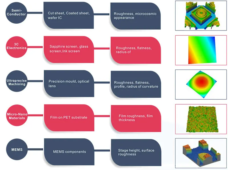
Whether you’re analyzing medical device surfaces, validating automotive components, or researching nanotechnology, this interferometer combines cutting-edge precision with intuitive operation. Its 3D surface mapping capability transforms complex geometries into actionable insights.
| Parameter | Base Model | Advanced Model | Pro Model |
|---|---|---|---|
| Measurement Resolution | 1 nm | +15% (0.85 nm) | +30% (0.7 nm)* |
| Scan Speed | 10 scans/min | 12 scans/min (+20%) | 15 scans/min (+50%) |
| Software Features | Basic analysis | Advanced algorithms | AI-driven analytics |
| Automation | Manual setup | Semi-automated | Fully automated |
Technical Breakthroughs:
Version Selection Guide:
With the Pro model’s 0.7 nm resolution, you can ensure flawless surface finishes for precision components. Its AI analytics paired with automated workflows cut downtime, delivering measurable ROI in high-volume production environments.

The Product Description is generated by third-party, and Alibaba.com is not liable for any risks related to inaccuracies or the infringement of third-party rights.
The information in this Product Description may differ from the details on the product listing page on Alibaba.com. Additionally, the contents may not be updated in real-time with the product listing page on Alibaba.com, and there may be delays in reflecting the most updated information. The description on product listing page takes precedence. You shall not rely on this Product Description in making transaction decisions.
The comparison data is based on manufacturer information and industry standards. Actual results may vary depending on individual use cases. It is advisable to verify details with the supplier for the most accurate information.