All categories
Featured selections
Trade Assurance
Buyer Central
Help Center
Get the app
Become a supplier
(993 products available)


 Ready to Ship
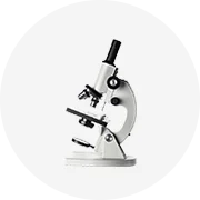
Microscopes are essential for PCB control to enhance the precision of the examination and repair of the circuits. Fresh Technology for PCB is also incorporated into the microscope to enhance efficiency and productivity. Here are the chief types of microscopes used in PCB control:
Optical Microscope
The most widely used type of microscope among the three is the optical microscope. Optical microscopes magnify their object by shining light on it and collecting the light through multiple lenses. It is instrumental for the physical inspection of printed circuit boards since it gives a clear image of the components at moderate magnification power.
Diana And The Microscope
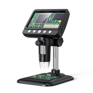
The digital microscope, which can be disconnect from any viewing screen, is gaining wide popularity day by day and especially among DIYers and hobbyists. This type of microscope comprises a camera system that captures the image, and the image is then relayed live on a screen or saved for future examination. A large variety of digital microscopes are available that vary greatly in their sizes, from small ones that attach to a computer to larger ones with their own display, and all for the purpose of image viewing.
Stereo Microscope
The stereo microscope is a type of optical microscope that provides a three-dimensional view of an object. This microscope has two optical paths to give depth perception, which makes it easy to handle large specimens on PCBs, such as components and solder joints. Stereo microscopes are widely used in assembly, quality control, and rework.
Compound Microscope
On the other hand, compound microscopes are fit for detailed investigations since they use multiple objective lenses to magnify a sample very finely. Because of their high-resolution capability, they are suited for inspecting small features on PCBs, such as micro soldering and fine traces. Compound microscopes are efficient for the quality control of PCBs and aid in detecting defects unnoticed by the bare eye.
Several Applications Of A Light Microscope
Another very modern PCB microscope is the microscope application that combines the conventional optical microscope with imaging technology. It is connected with imaging devices such as cameras; hence, images can be captured and analyzed for further review. The PCRP allows users to document detailed modifications and creates reports to improve efficiency.
USB Microscope
A form of digital microscope that connects to computers through a universal serial port is known as a USB microscope. It can be affordably purchased and is portable, but it has to be connected through a USB cable. For this reason, a USB microscope is a commonly used option for on-the-go professionals and enthusiasts. To enable one to do affordably and practically, the USB microscope connects easily with its computer for image capturing and processing.
PCB control microscopes need to have certain specifications and come with features to achieve and maintain their efficiency. These factors include:
Magnification Power
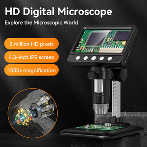
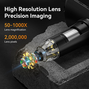
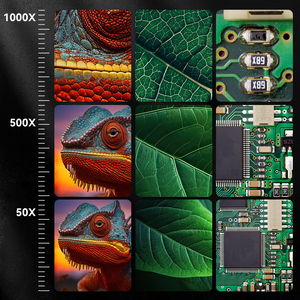
The magnification power is a critical specification of PCB control microscopes because it determines how much one will be able to see the components. PCB control microscopes should have a magnification range from 10x to 50x for composite inspections or solder joints and other fine work. It depends on the application, but several models have variable magnification to hold different PCB inspection needs.
Resolution
Resolving power is another specification relating to the power of a microscope to differentiate between close-together objects as distinct entities. It is essential in PCB control as it leads to the clarity of detail. High-definition imaging, whether optical or digital, is required to see micro-texts, for instance, on PCBs further and to give correct assessments.
Lighting System
There are inbuilt illumination systems in PCB microscopes, whereby LED lights are the most commonly used source, embedded in the objectives or around the stage. Good lighting is very important to get a clear picture and to see details on reflective surfaces, which is especially useful in PCB control. Lighting systems have adjustable brightness and various lighting modes, such as ring, transmitted, or reflected, to enhance flexibility.
Camera Integration
Many of the modern microscopes today that are used for PCB control come with a camera embedded within them or have the option to attach one. This feature makes it more convenient for users to capture images and share them easily with desktops or laptops. Most of these cameras have high-resolution images that are critical for documentation purposes.
Working Distance
There is a definition of working distance as the space between the objective lens and the specimen when focusing. This is especially important in the control of PCBs since it allows the technician to work easily while there are components under the PCB microscopes. A large working distance goes together with a greater depth of field, which is very helpful in making soldering repairs and adjusting components.
Software Features
Some microscopes have rather advanced software features for analysis and processing. Image measurement, annotation, and comparison software is embedded in microscopes for PCB control, which might also include defect detection algorithms. These software features improve the inspection process to help achieve high accuracy and efficiency during control applications.
Microscopes used for PCB control are different from each other, and their applications are based on their specific industries, which redefine inspections, repairs, and testing. They are commonly used in the following scenarios:
Quality Inspection
Microscopes are used in their primary application in the field of quality control, where they are instrumental in the detection of defects on PCBs. Printed circuit boards are subjected to solder joint examinations, component misalignment, and trace breakage. This is especially useful inPCB microscopy since it allows one to see detailed images and enhance the detection of defects before errors of greater magnitude are corrected.
Assembly and Manufacturing
PCB assembly operations require the use of microscopes to ensure the accurate placement of components and to get proper soldering performed. An inspector working in the assembly line may need to use magnification to see if surface-mounted devices are placed correctly or whether there is a cold solder joint. This leads to better accuracy and a reduction of errors.
Repair and Rework
The repair and rework of vehicles that have been employed for a long time requires a lot of help from PCB microscopes. The technician checks the problem on the circuit board through magnification to determine the best method of repair. This is used in areas like replacing components, fixing broken traces, and reworking solder joints, where the high level of accuracy is a demand.
Research and Development
Microscopes are very essential during the research and testing stages of a product's life cycle. In this case, for instance, PCBs go through a stage of stress-testing, component-safety evaluations, and material-analysis evaluation done under magnification at the microscope. This brings designers and engineers up close to their designs, giving them an insight that facilitates innovation and minimizes work.
Testing and Failure Analysis
PCB microscopies are employed in the diagnosis of electronic equipment to identify the problem and explain failure. PCB goes through examination under magnification to determine what leads to the malfunction, whether it is manufacturing defects, component failures, or material degradation. This is useful for evasion purposes and bringing out solutions to problems in future design and production.
The choice of a microscope for easy PCB control depends on various factors that relate to magnification, flexibility, operating distance, and lighting system. Consider the following while selecting:
Magnification and Zoom
For any and all inspections on PCBs, it is very critical to have optimum magnification and a good zoom range. The microscope used should come with several magnification levels to allow one to switch from general observations to detailed ones. A good option would be a microscope with a zoom function that offers a continuous magnification span.
Resolution and Clarity
This is the basis of the clarity of the image, which is necessary for detecting small components or solder joints. It is advised that high-resolution PCBs are to be used to get high-definition images as this will lead to detailed inspections. Ensure that the camera or optical system embedded in the microscope is capable of producing sharp, clear images during its use.
Lighting
A good lighting system is very necessary for an accurate inspection of circuits as it will help capture reflection on the circuits. Select a microscope with bright, adjustable lighting, especially those with LED illumination ring and depth of field, so as to avoid shadows. This will ensure proper visual of every detail on the PCB.
Working Distance
PCB inspections often involve the need for technicians to work on the board, especially while soldering or making adjustments. Go for a microscope with a sufficiently long working distance. Working distance and depth of field are considerable working distances, allowing one to work comfortably without interfering with the lens.
Portability and Design
Portability plays a significant role when micromotor cars are to be used in different areas, just like in field inspections. Get a light and compact design if mobility is particularly one of the advantages. Some Cctv microscopes come in stock that can be easily detached from the base and used as handheld for field.
Software and Analysis Tools
A number of microscopes come with different software options for analysis, such as image capturing, measurement, and documentation of inspected components. These features can help improve the inspection process and make it easier to keep records for future reference. Choosing a microscope that comes with good software for analysis will help one with effective PCB control.
Any microscope with optimum magnification range, good resolution, proper lighting, and working distance is a good choice for PCB control. These are the best since they provide detailed inspection of components and solder joints.
Generally, 10x to 50x magnifications are sufficient for the initial inspection of PCBs. However, going for more detailed work, types of equipment that offer variable magnifications are necessary.
LED lightings are the most effective and preferred for PCB inspections since they do not generate any heat and have an adjustable brightness setting. This helps avoid shadows and gives a clear view of the PCB.
Still, it is possible, but a failure or an improper placement of a high ep microscope will lead to inaccurate results and possibly damage to the circuit. It is always a good idea to use a microscope specially designed for PCB inspection to achieve great accuracy and detail.
No maintenance is required for the optical lens of the microscope, but a general care for cleanliness and good condition has to be part of a routine. The lens should always be kept clean to avoid distortion and a clear view of the inspected PCB.