N Type Semiconductor


 0
0


 1/3
1/3


 1/3
1/3


 1/3
1/3


 1/3
1/3

 CN
CN


 1/1
1/1


 0
0


 1/3
1/3


 1/6
1/6


 1/3
1/3


 1/5
1/5


 1/3
1/3


 1/3
1/3


 0
0
 0
0


 1/2
1/2


 1/8
1/8


 1/3
1/3
 CN
CN


About n type semiconductor
Where to Find N-Type Semiconductor Suppliers?
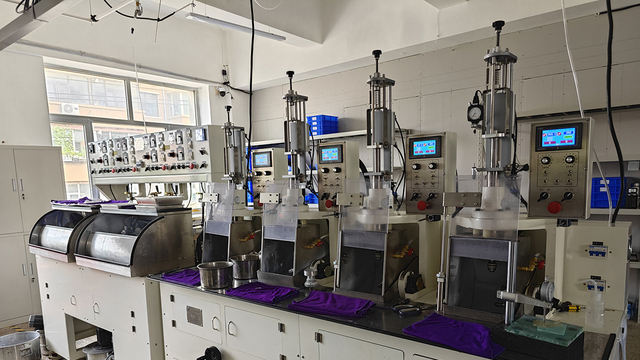
China leads global production of n-type semiconductors, with key manufacturing hubs concentrated in Jiangsu, Jilin, and Guangdong provinces. These regions host vertically integrated material science facilities specializing in silicon, silicon carbide (SiC), and bismuth telluride-based compounds. Changchun and Nantong serve as centers for IC-grade silicon wafers, leveraging proximity to research institutions and semiconductor fabrication clusters. Shenzhen and Shanghai have emerged as innovation zones for advanced substrates, including 4H-SiC and MEMS-grade materials used in high-power electronics and thermoelectric devices.
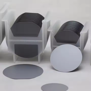
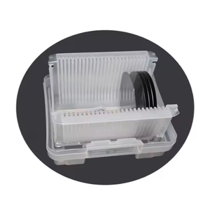
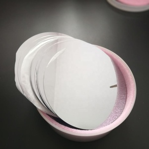
The industrial ecosystem supports diverse crystal growth techniques—such as Czochralski (CZ) and Bridgman methods—and wafer processing capabilities ranging from 1-inch to 8-inch diameters. Suppliers offer polished, double-sided, and customized-shape wafers tailored for photovoltaics, power modules, and sensor applications. Economies of scale enable competitive pricing, with entry-level 1-inch wafers available from $1.99/unit and bulk orders benefiting from localized supply chains that reduce logistics overhead by up to 25% compared to non-Asian manufacturers.
How to Choose N-Type Semiconductor Suppliers?
Evaluate suppliers using the following technical and operational benchmarks:
Material & Process Specifications
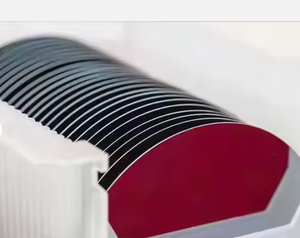
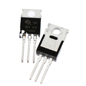
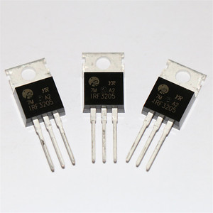
Confirm substrate type (e.g., monocrystalline silicon, SiC, Bi₂Te₃), doping concentration, resistivity range, and surface finish requirements. For power electronics, verify 4H-SiC polytype consistency and epitaxial layer quality. In thermoelectric applications, assess carrier mobility and Seebeck coefficient documentation.
Quality Management Systems
While formal ISO 9001 certification is not universally declared in available data, prioritize suppliers demonstrating structured quality control through:
- On-time delivery rates ≥96%
- Response times ≤6 hours
- Documented testing procedures for electrical and structural properties
Cross-reference product listings with reorder rates; values below 15% suggest limited post-sale issues or niche market positioning.
Production Flexibility and Scalability
Assess capacity based on minimum order quantity (MOQ) structures and unit scalability. Suppliers offering single-piece MOQs (e.g., 1 piece for $400–$2,000 SiC wafers) cater to R&D prototyping, while those requiring 10–25 pieces support pilot-line integration. Customization options—including diameter, thickness, orientation (100, 111), and polishing—are critical for application-specific designs.
What Are the Best N-Type Semiconductor Suppliers?
| Company Name | Main Materials | Wafer Diameter Range | Min. Order | Price Range (USD) | On-Time Delivery | Avg. Response | Reorder Rate | Revenue Tier |
|---|---|---|---|---|---|---|---|---|
| Changchun Elink Technology Co.,Ltd. | Silicon (IC Grade) | 1–8 inch | 10–20 pcs | $0.69–20.99 | 100% | ≤3h | <15% | $30K+ |
| Wellen Technology Co., Ltd. | Bismuth Telluride (Bi₂Te₃) | N/A (bulk crystals) | 1 kg | $299–386 | 98% | ≤6h | <15% | $50K+ |
| Nantong Ruisen Optical Co., Ltd. | Silicon, SiC | Up to 6 inch | 10 pcs | $0.50–10 | 100% | ≤6h | <15% | $4K+ |
| Shenzhen Sunhokey Electronics Co., Ltd. | Silicon Carbide (4H-N type) | 100mm (4 inch) | 5–10 pcs | $490–3,800 | 96% | ≤3h | 33% | $130K+ |
| Shanghai Xinkehui New Material Co., Ltd. | SiC, III-V Compounds, Silicon | 2–6 inch | 1–25 pcs | $25–2,000 | 100% | ≤5h | <15% | $20K+ |
Performance Analysis
Changchun Elink and Nantong Ruisen offer cost-effective solutions for standard silicon wafers with strong delivery reliability (100%) and low reorder rates, indicating stable performance for routine procurement. Wellen Technology specializes in thermoelectric materials, providing kilogram-scale Bi₂Te₃ ingots ideal for Peltier module fabrication. Shenzhen Sunhokey commands premium pricing for high-purity 4H-SiC substrates but exhibits a higher reorder rate (33%), suggesting potential demand volatility or customer acquisition focus. Shanghai Xinkehui stands out for flexibility, supporting single-unit sampling across multiple material systems—an advantage for early-stage development projects.
FAQs
How to verify n-type semiconductor supplier reliability?
Analyze delivery performance (target ≥96%), response speed (≤6h preferred), and transaction volume as proxies for operational stability. Request material test reports (MTRs) detailing dopant concentration, carrier density, and crystallinity. For mission-critical applications, conduct remote audits via facility walkthrough videos focusing on cleanroom standards and metrology equipment.
What is the typical lead time for n-type semiconductor samples?
Standard wafer samples ship within 7–15 days. Custom-doped or large-diameter substrates (e.g., 8-inch) may require 20–30 days due to crystal growth cycles. Thermoelectric ingot production typically takes 10–18 days depending on annealing schedules.
Can suppliers provide custom doping or orientation?
Yes, multiple suppliers list customizable resistivity, doping type (N/P), and crystallographic orientation (100, 111). Confirm availability of secondary processing such as backside metallization, SOI structuring, or passivation layers prior to order placement.
Are free samples available for evaluation?
Free samples are uncommon due to material costs. However, some suppliers credit sample fees against future bulk orders. Expect to pay full price for high-value substrates like 4H-SiC, where a single 100mm wafer can exceed $800.
What packaging and shipping methods are used?
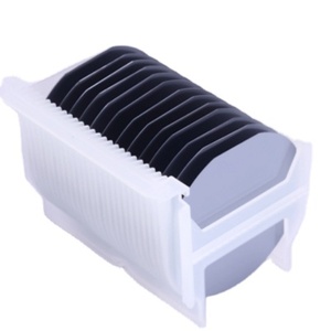
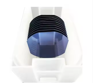
Wafers are shipped in sealed cassettes within anti-static containers under nitrogen atmosphere. Bulk crystals use padded vacuum-sealed packaging. Most suppliers support international express (DHL/FedEx) for small parcels and sea freight for containerized orders, with export documentation provided upon request.


