P Type Semiconductor


 0
0


 1/3
1/3


 1/3
1/3


 1/3
1/3


 1/3
1/3


 0
0


 1/3
1/3


 1/6
1/6


 1/3
1/3


 0
0


 0
0


 1/3
1/3


 1/3
1/3


 1/1
1/1


 1/3
1/3


 1/3
1/3


 1/1
1/1


 0
0

About p type semiconductor
Where to Find P-Type Semiconductor Suppliers?
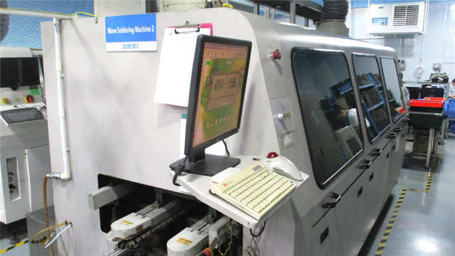
China remains a central hub for semiconductor material manufacturing, with key suppliers concentrated in specialized industrial zones focused on advanced materials and optoelectronics. Companies based in Changchun and Shanghai lead in silicon wafer and compound semiconductor substrate production, leveraging regional expertise in crystal growth and precision polishing. These clusters benefit from proximity to research institutions and electronics manufacturing centers, enabling rapid iteration and integration into downstream applications such as MEMS devices, power electronics, and photovoltaics.
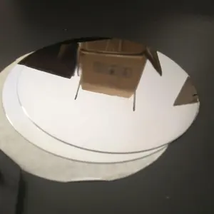
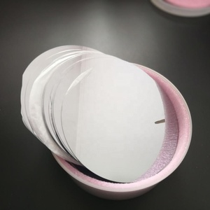
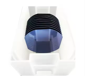
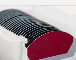
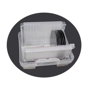
Suppliers offer a range of p-type semiconductor products, including single-crystal silicon wafers (2–8 inch), doped substrates, and custom-shaped SiC wafers. Production processes typically include Czochralski (CZ) or float-zone (FZ) crystal growth, followed by slicing, lapping, etching, and double-sided polishing. The presence of vertically integrated facilities allows control over doping concentration (e.g., boron-doped p-type) and resistivity ranges, critical for device performance. Buyers gain access to scalable output with lead times averaging 15–30 days for standard configurations, while customized orders may extend to 45 days depending on complexity.
How to Choose P-Type Semiconductor Suppliers?
Selecting reliable partners requires rigorous evaluation across technical, operational, and transactional dimensions:
Material & Process Specifications
Confirm substrate type (Si, SiC, InP), orientation (e.g., <100>, <111>), thickness tolerance (±10–50 µm), and surface finish (polished/epitaxial). For IC-grade materials, verify resistivity range compliance (e.g., 1–100 Ω·cm for p-type Si). Demand documentation on dopant uniformity and carrier concentration measurements via four-point probe or Hall effect testing.
Quality Assurance Systems
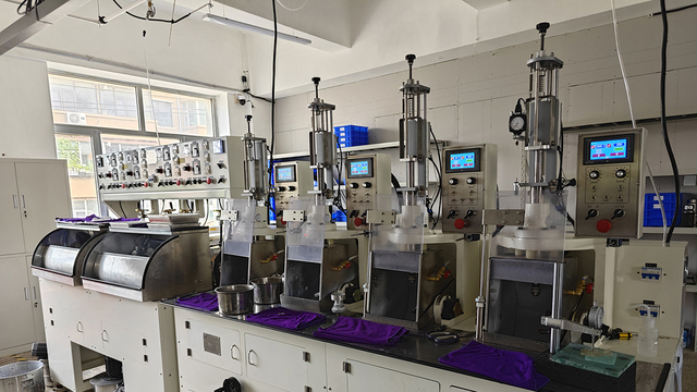
Prioritize suppliers adhering to ISO 9001 standards for quality management. While not all list certifications explicitly, consistent on-time delivery rates (>94%) and low reorder rates (<15% for three suppliers in the dataset) indicate stable production and customer satisfaction. Look for evidence of cleanroom fabrication environments and particle contamination controls essential for electronic-grade materials.
Production Capacity and Customization
Evaluate capability through available product range and minimum order quantities (MOQs). Key indicators include:
- Wafer diameter support up to 8 inches for mainstream CMOS compatibility
- Custom shaping, doping, and coating services (e.g., MEMS-grade double-sided polished wafers)
- Scalable MOQs ranging from 5 to 25 pieces for prototyping and pilot runs
- In-house metrology for dimensional and electrical validation
Cross-reference listed online revenue (up to US $130,000+) and response times (≤1–6 hours) as proxies for operational responsiveness and market engagement.
Transaction and Risk Mitigation
Utilize secure payment mechanisms and request sample testing before full-scale procurement. Assess supplier reliability through verifiable performance metrics: on-time delivery (three suppliers report 100%), response speed, and post-purchase support. For high-value components like 12-inch silicon electrodes or III-V compound substrates, insist on batch traceability and certificate of conformance (CoC).
What Are the Best P-Type Semiconductor Suppliers?
| Company Name | Main Products | Online Revenue | On-Time Delivery | Response Time | Reorder Rate | Min. Order Quantity | Price Range (USD) |
|---|---|---|---|---|---|---|---|
| Changchun Elink Technology Co.,Ltd. | Silicon wafers, MEMS-grade substrates | US $30,000+ | 100% | ≤3h | <15% | 10–20 pcs | $0.69–$20.99 |
| Nantong Ruisen Optical Co., Ltd. | Silicon wafers, SiC substrates | US $4,000+ | 100% | ≤6h | <15% | 10 pcs | $0.50–$10 |
| Changchun Yutai Optics Co.,ltd | N/P-type silicon wafers, 2–8 inch | US $130,000+ | 94% | ≤1h | 27% | 5–25 pcs | $8–$68 |
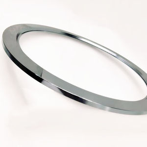
| Dalian King Choice Non-Ferrous Metals Products Co., Ltd. | Silicon electrodes, focusing rings | Not specified | 100% | ≤2h | Not available | 1 pc | $1,000–$2,500 |
| Shanghai Xinkehui New Material Co., Ltd. | Sic wafers, III-V substrates, InP | US $20,000+ | 100% | ≤6h | <15% | 1–25 pcs | $2.50–$900 |
Performance Analysis
Changchun Yutai stands out with the highest reported online revenue (US $130,000+), sub-hour response time, and broad diameter coverage (2–8 inch), making it suitable for volume buyers requiring fast communication. Changchun Elink and Nantong Ruisen offer competitive pricing for small-batch procurement, with MOQs starting at 10 pieces and prices as low as $0.50/unit. Dalian King Choice specializes in high-value consumables like p-type silicon electrodes, targeting OEMs in semiconductor equipment maintenance. Shanghai Xinkehui provides access to advanced materials such as InP and SiC, albeit at higher price points reflecting niche application demands. Suppliers with 100% on-time delivery and response times under 3 hours demonstrate strong operational discipline—critical for just-in-time supply chains.
FAQs
How to verify p-type semiconductor material specifications?
Request detailed datasheets including crystal orientation, resistivity, thickness, TTV (Total Thickness Variation), and dopant type (e.g., boron). Validate using independent testing methods such as SIMS (Secondary Ion Mass Spectrometry) or sheet resistance mapping.
What is the typical lead time for p-type wafer orders?
Standard wafer shipments take 15–30 days after order confirmation. Customized substrates (non-standard sizes, special doping profiles) may require 30–45 days. Expedited processing is occasionally available upon negotiation.
Can suppliers provide samples for qualification?
Yes, most suppliers accommodate sampling with MOQs as low as 1–10 pieces. Sample costs typically reflect full unit pricing, though some waive fees for subsequent bulk orders. Confirm if samples are representative of mass production batches.
Are p-type semiconductors RoHS compliant?
Most silicon-based p-type wafers are inherently RoHS-compliant. However, confirm absence of restricted substances in packaging, coatings, or handling materials, especially for export to EU or North American markets.
What customization options are available?
Common customizations include specific resistivity tuning, beveling, laser marking, and backside metallization. Advanced requests such as epitaxial layer deposition or MEMS-compatible surface finishes require suppliers with dedicated R&D infrastructure—verify capabilities through technical consultations.


