Printed Circuit Board Semiconductor


About printed circuit board semiconductor
Where to Find Printed Circuit Board Semiconductor Suppliers?
China remains the global epicenter for printed circuit board (PCB) and semiconductor manufacturing, with Shenzhen emerging as a dominant hub due to its concentrated electronics ecosystem. The city hosts a dense network of specialized PCB fabricators, semiconductor packaging facilities, and design houses, enabling rapid prototyping and scalable production. This clustering reduces component sourcing lead times by up to 40% compared to decentralized regions, while proximity to Tier-1 contract manufacturers ensures alignment with industry standards.
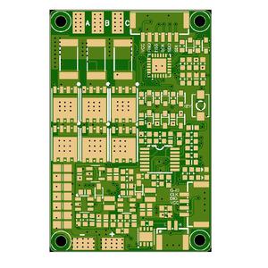
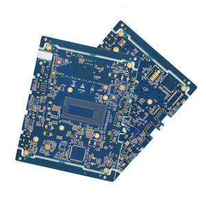
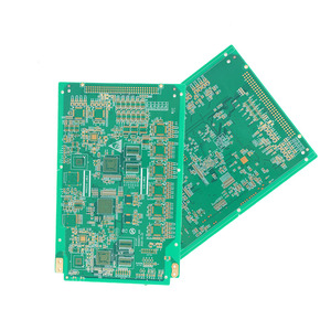
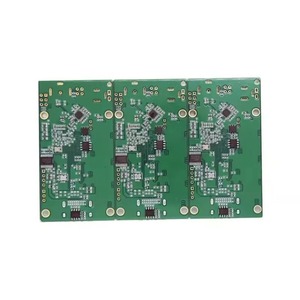
The region’s infrastructure supports full-spectrum capabilities—from single-layer boards to high-density interconnect (HDI) and multilayer PCBs used in advanced semiconductor testing. Suppliers leverage automated optical inspection (AOI), impedance-controlled routing, and precision etching to meet tight tolerances required in probe cards, burn-in boards, and optical transceiver modules. Buyers benefit from integrated services including Gerber file validation, 3D previews, and turnkey PCBA assembly, streamlining time-to-market for complex electronic systems.
How to Choose Printed Circuit Board Semiconductor Suppliers?
Effective supplier selection requires rigorous evaluation across technical, operational, and transactional dimensions:
Technical & Process Compliance
Verify adherence to IPC-6012 Class 2 or Class 3 standards for PCB fabrication, particularly for applications requiring high reliability. For semiconductor-related PCBs—such as ATE (Automated Test Equipment) or probe cards—demand evidence of controlled impedance design, microvia processing, and thermal stability under repeated cycling. RoHS and REACH compliance is standard; ISO 9001 certification indicates structured quality management systems.
Production Capacity Assessment
Evaluate key indicators of scalability and consistency:
- Minimum facility size of 2,000m² for stable batch processing
- In-house capabilities covering PCB lamination, drilling, plating, and SMT assembly
- Dedicated engineering support for HDI, heavy copper, and high-frequency materials
Cross-reference on-time delivery rates (>95%) and response times (≤5 hours) with order volume history to assess operational maturity.
Procurement Risk Mitigation
Prioritize suppliers offering transparent pricing structures with clear MOQ breakdowns. Utilize secure payment frameworks where funds are released post-inspection. Request sample batches to validate solder mask accuracy, trace width consistency, and layer registration before scaling. Confirm export experience with documentation prepared for customs clearance in target markets.
What Are the Best Printed Circuit Board Semiconductor Suppliers?
| Company Name | Main Products | Monthly Output (Listings) | On-Time Delivery | Reorder Rate | Avg. Response | Online Revenue | Customization Options | Min. Order Quantity |
|---|---|---|---|---|---|---|---|---|
| Shenzhen Keshijia Electronic Precision Co., Ltd. | Multilayer PCB, Heavy Copper PCB, High Frequency PCB | 231+ | 100% | <15% | ≤5h | US $600+ | Design & Assembly | 1–2 pieces |
| Shenzhen Fengchengda Technology Co., Ltd. | PCBA, Multilayer PCB, FPC | 353+ | 66% | 50% | ≤2h | US $3,000+ | Custom Testing PCB | 1 piece |
| ShenZhen Nova Semiconductor Co., Ltd. | HDI, Multilayer PCB, OEM/ODM PCBA | 5+ | 98% | 32% | ≤3h | US $100,000+ | Gerber Review, 3D Preview, PCBA | 1 piece |
| Shenzhen Ac Electronic Technology Co., Ltd. | Other PCB & PCBA, HDI | 485+ | 100% | 25% | ≤3h | US $140,000+ | Limited | 1–2 sqm |
| Shenzhen Yongchangtai Electronics Co., Ltd. | Custom PCB, 94v0 PCBA | 5+ | 100% | <15% | ≤2h | US $1,000+ | Color, Size, Logo, Packaging | 100 pieces |
Performance Analysis
ShenZhen Nova Semiconductor and Shenzhen Ac Electronic stand out in revenue scale and delivery reliability, both maintaining near-perfect on-time performance despite high transaction volumes. Nova excels in customization depth, offering Gerber analysis and 3D modeling—critical for complex semiconductor interface designs. In contrast, Shenzhen Fengchengda shows strong customer retention (50% reorder rate), suggesting competitive service quality despite lower delivery consistency. Keshijia and Yongchangtai offer ultra-low MOQs ideal for prototyping, though Yongchangtai’s 100-piece minimum reflects economies geared toward mid-volume runs. Buyers seeking HDI or high-frequency boards should prioritize suppliers with demonstrated expertise in impedance control and fine-line lithography.
FAQs
How to verify printed circuit board semiconductor supplier reliability?
Cross-check self-reported certifications with third-party verification platforms. Request process audit trails including AOI reports, peel strength tests, and thermal cycling data for critical applications. Analyze buyer feedback focusing on defect rates, communication clarity, and post-delivery support.
What is the typical lead time for custom PCBs?
Standard multilayer PCB prototypes take 5–7 days. HDI or buried-via designs require 10–14 days. Full PCBA with component sourcing extends timelines to 15–20 days. Rush services may reduce this by 3–5 days at premium cost.
Can suppliers handle small-batch and prototype orders?
Yes, most Shenzhen-based suppliers accommodate orders as low as one piece, particularly for bare PCBs. However, unit costs decrease significantly at 100+ units. Confirm whether panelization or shared tooling affects turnaround and yield.
Do manufacturers provide free samples?
Sample policies vary. Some suppliers waive fees for qualified buyers placing follow-up orders. Others charge nominal fees covering material and setup, typically refundable against future production runs exceeding 500 units.
How to initiate customization for semiconductor test boards?
Submit detailed specifications including layer count, dielectric material (e.g., FR-4, Rogers), via structure, surface finish (ENIG, immersion silver), and electrical requirements such as current load and signal integrity. Reputable partners will return stack-up diagrams and impedance calculations within 48 hours.


