
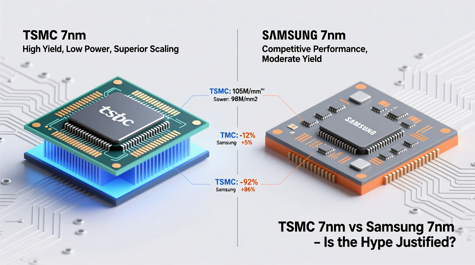
When it comes to advanced semiconductor manufacturing, few names command as much attention as TSMC and Samsung. Both companies have pushed the boundaries of chip fabrication with their 7nm process nodes, powering everything from flagship smartphones to high-performance computing systems. But amid widespread praise for TSMC’s 7nm technology, a critical question arises: Is the dominance of TSMC truly deserved, or has marketing overshadowed technical reality? This article dives deep into the engineering, performance, power efficiency, and real-world applications of both foundries’ 7nm offerings to determine whether the hype is justified.
Understanding the 7nm Node: More Than Just a Number
The term “7nm” refers nominally to the smallest feature size on a chip, but in modern semiconductor manufacturing, it no longer reflects physical dimensions. Instead, it serves as a marketing label indicating a generational improvement over previous nodes like 10nm or 14nm. What matters more than the number are metrics such as transistor density, power consumption, performance at voltage (PPA), yield rates, and manufacturability.
TSMC and Samsung each developed their own version of 7nm, leveraging different materials, design rules, and lithography techniques. While both claim similar advancements, subtle differences in execution lead to divergent outcomes in actual product deployment.
Transistor Density and Scaling Efficiency
One of the most telling indicators of process quality is transistor density — how many transistors can be packed per square millimeter. Higher density allows for smaller dies, lower costs, and improved performance due to shorter interconnects.
| Foundry | Process Node | Transistor Density (MTr/mm²) | Lithography Used |
|---|---|---|---|
| TSMC | N7 | 91.2 | Deep UV (ArF immersion) |
| Samsung | 7LPP | 88.5 | Deep UV (ArF immersion) |
| TSMC | N7+ | 100.8 | First EUV layer |
| Samsung | 7LPE | 80.0 | Deep UV only |
As shown above, TSMC’s standard N7 node already held a slight edge in density over Samsung’s initial 7LPP (Low Power Plus) offering. However, TSMC’s enhanced N7+ process, which introduced extreme ultraviolet (EUV) lithography for critical layers, further widened the gap. Samsung later adopted EUV in its 6nm and refined 7nm variants, but early momentum favored TSMC.
Performance and Power Efficiency: Real-World Benchmarks
Density alone doesn’t tell the full story. The true test lies in how efficiently these processes translate into real silicon. Consider Apple’s A13 Bionic, fabricated on TSMC’s N7P (an evolution of N7), versus Qualcomm’s Snapdragon 865, made on Samsung’s 7LPP.
- The A13 delivered higher peak CPU performance while consuming less power under load.
- In GPU-intensive workloads, the A13 maintained cooler temperatures and sustained clock speeds longer.
- Benchmarks from AnandTech showed that the A13 achieved up to 30% better performance-per-watt than competing Android SoCs of the same era.
This advantage wasn’t solely due to Apple’s chip design prowess—it was amplified by TSMC’s superior process control, lower leakage current, and tighter binning tolerances.
“TSMC’s process consistency allows us to push frequency limits without sacrificing battery life.” — Anonymous Senior SoC Architect, Mobile Chip Designer
Leakage Current and Thermal Behavior
One area where Samsung initially struggled was managing leakage current at scale. Due to slightly less mature finFET structures and gate oxide uniformity, early Samsung 7nm chips exhibited higher static power draw, especially at elevated temperatures. This meant devices would throttle sooner during sustained workloads.
In contrast, TSMC’s process refinements allowed for tighter threshold voltage control, enabling dynamic voltage and frequency scaling (DVFS) to operate more effectively. As a result, TSMC-based chips could maintain high performance states longer before thermal throttling kicked in.
Yield Rates and Manufacturing Maturity
Even the best-designed process means little if it can’t be manufactured reliably at scale. Yield rate—the percentage of functional dies per wafer—is a key competitive metric. High yields reduce cost and increase supply stability.
Reports from industry analysts at TechInsights and SemiAnalysis indicated that TSMC achieved >80% yield on its N7 process within six months of ramping production. Samsung, meanwhile, reportedly took nearly twice as long to reach comparable yields on 7LPP, impacting delivery timelines for clients like NVIDIA and IBM.
This maturity gave TSMC a decisive edge in attracting premium customers. AMD shifted entirely to TSMC for its Zen 2 architecture (e.g., Ryzen 3000 series), citing not just performance gains but also confidence in volume availability. Meanwhile, Samsung struggled to retain major external clients beyond Qualcomm and its own Exynos line.
Case Study: AMD’s Shift from GlobalFoundries to TSMC
In 2019, AMD launched its third-generation Ryzen processors based on Zen 2 microarchitecture. These were the first desktop CPUs built on TSMC’s 7nm node. Compared to the previous generation (12nm GlobalFoundries), the new chips offered:
- Up to 50% more instructions per cycle (IPC).
- Higher core counts (up to 16 cores/32 threads) without excessive die sizes.
- Lower TDP despite increased performance.
The success wasn’t just architectural—it was enabled by TSMC’s ability to deliver dense, efficient, and scalable 7nm wafers consistently. Had Samsung been the sole alternative at the time, AMD may have faced delays or compromised designs.
Design Flexibility and Ecosystem Support
Beyond raw physics, a foundry’s value includes its design ecosystem: IP libraries, reference flows, EDA tool integration, and support for complex designs like multi-die chiplets.
TSMC invested heavily in building robust design infrastructure around its 7nm node. It partnered closely with Synopsys, Cadence, and Mentor (Siemens) to ensure sign-off accuracy and timing closure. This reduced risk for fabless companies designing billion-transistor SoCs.
Samsung, while improving rapidly, lagged in ecosystem maturity. Some designers reported longer turnaround times for design rule checks (DRC) and layout-vs-schematic (LVS) verification, slowing development cycles.
FAQ: Common Questions About TSMC vs Samsung 7nm
Does Samsung’s 7nm use EUV?
Samsung’s original 7LPP did not use EUV lithography; it relied entirely on deep ultraviolet (DUV). TSMC introduced EUV in its enhanced N7+ variant, giving it finer patterning and fewer mask layers. Samsung incorporated EUV starting with its 6nm node and later refined versions of 7nm.
Are there any advantages to Samsung’s 7nm?
Yes. Samsung offered competitive pricing and favorable terms to attract early clients. Additionally, Samsung’s gate-all-around (GAA) research pipeline suggests stronger long-term scalability beyond 3nm, potentially closing the gap in future nodes.
Can consumers notice the difference between TSMC and Samsung 7nm chips?
Indirectly, yes. Devices using TSMC’s 7nm often exhibit better battery life, sustained performance, and cooler operation. For example, iPhone models consistently outperformed contemporaneous Android flagships in Geekbench and GFXBench tests, partly due to the underlying process advantage.
Actionable Checklist for Evaluating Foundry Choices
- Verify the exact process variant: Distinguish between base 7nm, EUV-enhanced, and derivative nodes (e.g., N7P, 7LPP).
- Assess yield and availability: Confirm production capacity and historical reliability.
- Analyze PPA metrics: Compare performance, power, and area against your design goals.
- Evaluate ecosystem tools: Ensure compatibility with your EDA flow and design team experience.
- Review client track record: Look at which major companies chose the process and why.
Conclusion: The Hype Is Largely Justified—But Not Absolute
TSMC’s leadership in the 7nm era is not merely a product of marketing hype. Measurable advantages in transistor density, power efficiency, yield rates, and ecosystem maturity contributed to tangible benefits for end users. From Apple’s A-series chips to AMD’s resurgence in CPUs and GPUs, TSMC-powered silicon consistently set new benchmarks.
That said, Samsung’s 7nm process was far from inadequate. It powered successful products and demonstrated the company’s growing capabilities. However, minor deficiencies in leakage control, yield stability, and design support limited its appeal to top-tier innovators seeking maximum headroom.
The broader takeaway is this: In semiconductor manufacturing, small margins compound into significant real-world differences. TSMC didn’t win because of one breakthrough—it won through consistent execution, relentless refinement, and strategic investment in every layer of the fabrication stack.


 浙公网安备
33010002000092号
浙公网安备
33010002000092号 浙B2-20120091-4
Comments
No comments yet. Why don't you start the discussion?