Wafer Processing Semiconductor


 Top sponsor listing

 CN
CN


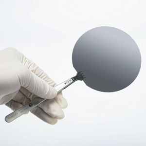


About wafer processing semiconductor
Where to Source Wafer Processing Semiconductor Suppliers?
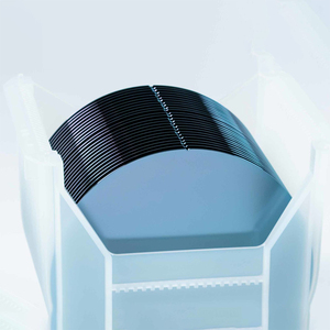
China leads in semiconductor wafer processing supply, with key manufacturing clusters in Jiangsu, Jilin, and Guangdong provinces offering specialized capabilities. Jiangsu-based suppliers leverage proximity to Shanghai’s microelectronics R&D hubs, enabling rapid iteration on advanced materials and thin-film substrates. Changchun in Jilin Province hosts legacy semiconductor fabrication expertise, particularly in silicon and compound wafers for IC-grade applications. Guangdong suppliers, centered in Guangzhou, focus on high-end equipment for wafer grinding, polishing, and thermal processing, supported by regional automation and precision engineering ecosystems.
These industrial zones provide vertically integrated production networks—spanning raw material sourcing, crystal growth, epitaxy, and final packaging—reducing component procurement lead times by 25–40% compared to non-cluster regions. Buyers benefit from concentrated technical labor pools, localized testing facilities, and streamlined logistics, achieving average order fulfillment cycles of 15–30 days for standard wafers and 45–60 days for custom equipment. Cost efficiencies range from 18–35% due to reduced overhead and bulk material access, particularly for 6-inch, 8-inch, and 12-inch wafer formats.
How to Evaluate Wafer Processing Semiconductor Suppliers?
Implement structured assessment protocols to ensure technical and operational reliability:
Material & Process Compliance
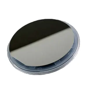
Confirm alignment with SEMI standards for wafer flatness, resistivity, and particle contamination. For electronic-grade applications, verify use of high-purity 4H-SiC, N-type/P-type silicon, and epitaxial deposition techniques. Demand documentation on doping concentration, crystal orientation (e.g., <100>, <111>), and surface finish (polished, etched, or epitaxial). RoHS and REACH compliance is essential for export markets.
Production Capacity Verification
Assess core competencies through measurable indicators:
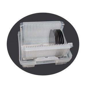
- Minimum 100+ monthly units for wafer carriers, rings, and storage systems
- In-house crystal growth and slicing capability for substrate manufacturers
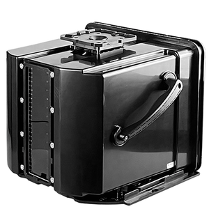
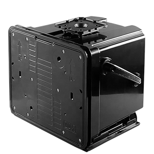
- CNC machining, vacuum coating, or RTP (Rapid Thermal Processing) integration for advanced processing
Cross-reference online revenue data and reorder rates: suppliers with consistent US $30,000+ digital sales typically maintain stable output and quality control.
Transaction & Quality Assurance
Prioritize partners with 100% on-time delivery records and response times under 5 hours, indicating operational responsiveness. Use sample testing to validate claims—benchmark wafer thickness uniformity (±1μm tolerance) and electrical performance against datasheets. For capital equipment, require factory acceptance tests (FAT) via video inspection before shipment. Escrow payment terms mitigate risk for high-value orders exceeding $50,000.
What Are the Leading Wafer Processing Semiconductor Suppliers?
| Company Name | Main Products | Listings | On-Time Delivery | Response Time | Reorder Rate | Revenue Tier | Key Offerings |
|---|---|---|---|---|---|---|---|
| Nantong Ruisen Optical Co., Ltd. | Optical Filters, Semiconductors | 484 | 100% | ≤5h | <15% | US $7,000+ | High-purity optical components with limited semiconductor wafer listings |
| Harbin Keyou Semiconductor Industry Equipment And Technology Research Institute Co., Ltd. | Other Inorganic Chemicals, Furnaces | 23 | 100% | ≤9h | - | - | High-purity 4H-N SiC wafers (6” and 8”), dummy wafers for process calibration |
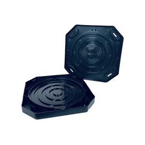
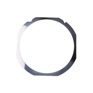
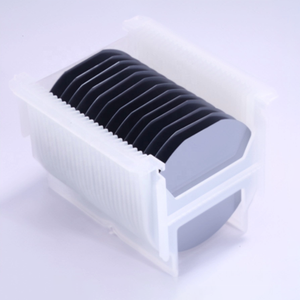
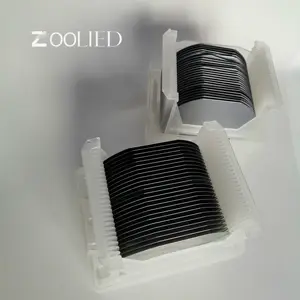
| YJ STAINLESS CO., LTD. | Semiconductors, Accessories | 162 | 100% | ≤4h | - | - | 300mm/12-inch wafers, stackable storage, film rings, metal components |
| Changchun Elink Technology Co.,Ltd. | Other Fabrication Services | 439 | 100% | ≤4h | <15% | US $30,000+ | IC-grade N/P wafers (1” to 4”), MEMS substrates, low-cost entry-level options |
| Guangzhou Minder-Hightech Co., Ltd. | Custom Semiconductor Equipment | 5 | 50% | ≤5h | 80% | US $280,000+ | Fully automated wafer manufacturing lines, CMP devices, RTP systems ($40k–$1M) |
Performance Analysis
YJ STAINLESS and Changchun Elink deliver strong value for consumable wafer components, combining fast response times with 100% delivery performance and competitive pricing (as low as $0.69/unit for MEMS-grade wafers). Harbin Keyou specializes in high-purity silicon carbide substrates critical for power electronics, though limited transaction transparency affects risk assessment. Guangzhou Minder-Hightech targets capital equipment buyers with full-line automation solutions, evidenced by high reorder rates (80%) despite lower delivery reliability (50%). Prioritize suppliers with documented customization options—such as laser marking, dimensional tuning, or packaging—for specialized integration. For volume wafer procurement, favor entities with diversified product portfolios and verified scalability.
FAQs
How to verify wafer material specifications?
Request certificates of analysis (CoA) detailing crystal structure, dopant type, carrier concentration, and total thickness variation (TTV). Cross-check batch numbers with production logs. For SiC wafers, confirm polytype consistency (4H vs. 6H) using X-ray diffraction reports.
What are typical MOQs and lead times?
Standard wafers: MOQs range from 1–10 pieces (samples) to 100+ for production runs. Lead time averages 10–20 days. Equipment orders require 45–75 days depending on complexity. Custom tooling may extend timelines by 2–3 weeks.
Do suppliers support OEM/ODM customization?
Yes. Common options include size modification (6”, 8”, 12”), surface treatment (polished, as-cut), labeling, and private branding. Guangzhou Minder-Hightech offers full system reconfiguration for thermal and chemical-mechanical processing tools.
Are samples available for evaluation?
Most suppliers offer paid samples. Expect costs between $50–$500 depending on wafer type. Sample fees may be credited toward first bulk orders. For equipment, virtual demonstrations substitute physical sampling.
What logistics options exist for international shipping?
Air freight is standard for wafers and small components (3–7 days globally). Sea freight applies to heavy machinery (20–35 days). Confirm FOB origin terms and insurance coverage. Ensure anti-static, vacuum-sealed packaging for sensitive materials.


